News: Microelectronics
9 January 2025
Fast gallium oxide MOCVD growth
Ohio State University (OSU) in the USA reports on increasing the growth rate for gallium oxide (β-Ga2O3) epitaxy using metal-organic chemical vapor deposition (MOCVD) [Dong Su Yu et al, Appl. Phys. Lett., v125, p242106 2024]. In particular, the team studied the effect of modifying the oxygen precursor and using off-axis substrates.
The researchers comment: “Results from this work provide guidance on MOCVD development of high-crystalline-quality β-Ga2O3 films for vertical power electronics.”
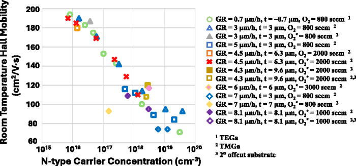
The resulting films, grown at 4.5μm/h, showed electron mobilities up to 190cm2/V-s at low 7x10¹⁵/cm3 carrier concentration, as needed in drift layers in high-power/high-voltage vertical devices, such as transistors and Schottky barrier diodes. The ultrawide bandgap (UWBG) of β-Ga2O3 also makes it attractive for ultra-violet (UV) solar-blind photodetectors.
The team reports: “Among several UWBG semiconductor candidates, such as aluminium nitride (AlN), diamond, and boron nitride (BN), β-Ga2O3 has a unique advantage of the availability of high-quality bulk Ga2O3 synthesized with low density of defects from melt growth techniques.”
MOCVD is attractive for β-Ga2O3 over faster halide vapor phase epitaxy (HVPE) in terms of resulting in smoother surface with fewer defects. HVPE films thus require further process steps such as chemical mechanical planarization (CMP). HVPE growth rates typically exceed 5μm. The OSU work has demonstrated good performance from MOCVD growth rates of 4.5μm/h, approaching the results of 3μm/h MOCVD.
The epitaxial β-Ga2O3 was grown on commercial semi-insulating (010) iron-doped β-Ga2O3 substrates. The substrates, with and without a 2° off-cut angle, were supplied by Novel Crystal Technology Inc. The Ga precursor was trimethyl-gallium (TMGa). For the oxygen component, the researchers compared the use of high-purity (>99.9999%) oxygen (O2), and the use of oxygen with 10 parts per million water molecules (O2*). The carrier gas was argon. The growth temperature and pressure were 950°C and 60Torr, respectively.
The growth rates ranged from 4.3μm/h to 8.1μm/h, depending on the precursor flow rates. Silane (SiH4) was used for n-type doping with silicon.
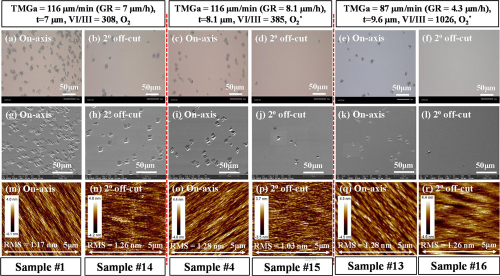
One effect of using O2* was to reduce the size and density of 3D pyramid-shaped surface defects, compared with high-purity O2. However, the O2* samples did have “a relatively high density of surface structures with much smaller feature sizes”.
Based on previous work, the researchers suggest that the presence of H in O2* MOCVD reaction increases the mobility of the adatoms on the substrate surface, increasing diffusion length, “leading to smoother and more uniform film surfaces”. The surface roughness with O2* was 1.48nm, compared with 2.59nm for a sample grown using high-purity O2.
Two on-axis samples with 6.3μm films (4.5μm/h growth) showed similar electron transport characteristics: 1.3x10¹⁶/cm3 and 1.4x10¹⁶/cm3 electron carrier concentration, and 185cm2/V-s and 180cm2/V-s mobility, for O2* and O2, respectively.
The researchers comment: “As the film thickness reduces, one should expect a more prominent influence of the surface or interface roughness on the transport properties. Future investigation is still required to understand the impact of the surface morphology on device performance. In particular, for devices with thick epitaxial layers, additional optimization of surface morphology may still be necessary.”

Figure 1: Surface views in optical, field emission scanning electron microscope (FESEM), and atomic force microscope (AFM) images of β-Ga2O3 epi-films grown on 2° off-cut and on-axis (010) semi-insulating β-Ga2O3 substrates under varied growth conditions (μm/min=μmol/min).
The use of 2° off-cut substrates further improved the surface morphology (Figure 1). The researchers comment: “The introduction of an off-cut angle on β-Ga2O3 substrates provides preferred nucleation sites for incoming Ga adatoms along the steps/edges, which suppresses the random nucleation sites and the formation of 3D defects. Furthermore, the use of O2* and relatively high V/III ratio result in optimal surface smoothness.”
High oxygen flow rates were also found to suppress carbon incorporation, according to secondary-ion mass spectroscopic analysis. Carbon tends to reduce the effectiveness and accuracy of silicon n-type doping due to severe charge compensation effects.

Figure 2: Comparison of room-temperature Hall mobility data for (010) β-Ga2O3 epi-films grown using TMGa with fast growth rates (4.3–8.1μm/h) versus electron concentration from OSU’s latest and previously reported data from MOCVD with TMGa and triethyl-Ga (TEGa) precursors.
The researchers achieved low controllable n-type doping with 7x10¹⁵/cm3 carrier concentration and 190cm2/V-s mobility (Figure 2). The growth rate was 4.5μm/h, and the performance was close to the ~200cm2/V-s record achieved with a slower growth of 3μm/h. These values are also close to the theoretical limit. The highest electron carrier concentration achieved was 3.6x18/cm3.
Gallium oxide MOCVD HVPE UV solar-blind photodetectors
The author Mike Cooke is a freelance technology journalist who has worked in the semiconductor and advanced technology sectors since 1997.


