


News: Microelectronics
30 January 2025
GaN complementary logic circuit building blocks
Researchers based in China claim “breakthrough” performance for complementary logic (CL) circuits based on gallium nitride field-effect transistors (FETs) in work presented at the International Electron Devices Meeting in December 2024 [Teng Li et al, IEDM session 16-1, 2024].
The team from Peking University, Beijing University of Technology, University of Science and Technology of China, and Hong Kong University of Science and Technology, comments: “The work demonstrates the potential of GaN complementary logic for MHz power integrated circuits (PICs) and harsh-environment electronics.”
A key bottleneck for GaN complementary logic performance is the p-channel FET complement to the well-established n-FETs. The maximum drain current of GaN p-FETs is typically less than 10mA/mm. This is related to the poor performance of magnesium (Mg) as an electron acceptor for creating positive hole charge carriers.
To overcome this problem, the researchers used epitaxial material with an aluminium nitride (AlN) layer inserted into the p-type layers. This created a charge polarization field that modified the Fermi level in the p-type layers, enhancing the Mg acceptor ionization.
The researchers explain: “The p-FET features an AlN insertion layer that pushes the acceptor energy level (EMg) to below the Fermi level (EF), so the holes from the EMg levels become fully ionized and are transferred to above the AlN.”
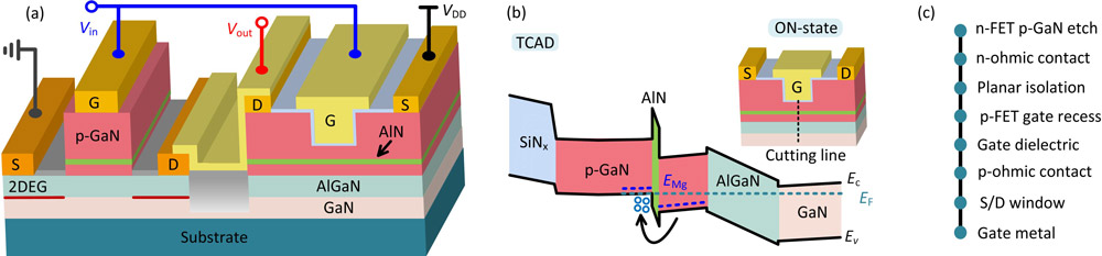
Figure 1: (a) GaN complementary logic (CL) platform scheme. (b) Simulated energy-band diagram of p-FET gate region in on-state. (c) Process flow.
The epitaxial structure used for the circuit fabrication (Figure 1) consisted of 200nm GaN, 13nm AlGaN barrier layer, 10nm p-GaN, 1.5nm AlN insertion layer, and 60nm p-GaN on GaN-on-sapphire substrate wafer.
The n-FETs were fabricated by etching through the p-type layers and making source/drain contacts with the n-type two-dimensional electron gas (2DEG) channel that forms below the AlGaN barrier. The annealed metals used for the ohmic contacts were titanium/aluminium/nickel/gold (Ti/Al/Ni/Au).
Planar device isolation was achieved using fluorine ion implantations at multiple energies.
The p-FET side of the complementary logic was fabricated with recessed gate and 20nm silicon nitride gate insulation. The ohmic source/drain contacts in this case were annealed Ni/Au. The final metalization was Ti/Au for the gate electrodes and probe pads.
The gates for both device types were centrally placed between the source and drain electrodes. The p-FET and n-FET gate lengths were 2μm and 4μm, respectively, with corresponding spacings for the source/drain of 4μm and 3μm.
Single p-FETs achieved maximum drain currents of 23mA/mm. The threshold voltage (Vth) was −0.5V, giving enhancement (E)-mode, ‘normally-off’ operation. The on/off current ratio was 6.5x10⁷. The sub-threshold swing was 89mV/decade. The n-FET was also E-mode with +1.3V threshold.
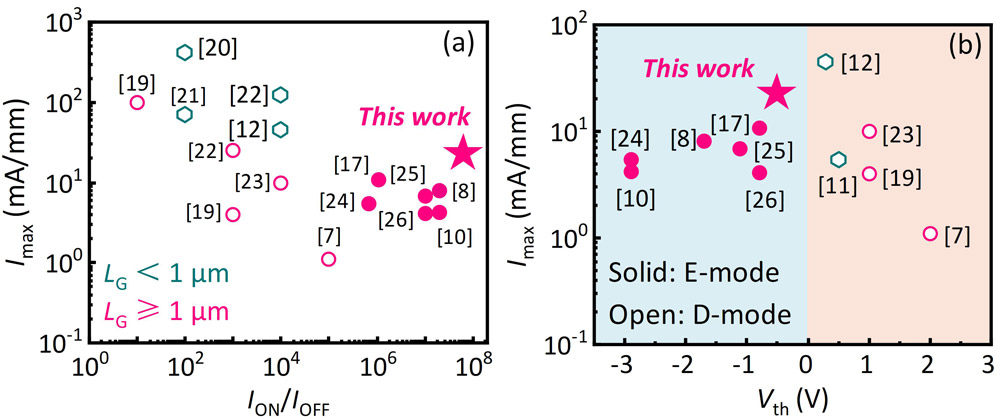
Figure 2: Benchmark of GaN p-FET (FinFETs and/or tri-gate FETs not included). Vth determined by 10μA/mm drain current for fair comparison.
Based on benchmark plots against published work (Figure 2), the team claims “superior Imax and ION/IOFF among E-mode GaN p-FETs”. Since the research was targeted at power IC deployment, the benchmark excluded FinFETs and trigate structures, which are aimed at high-speed/radio frequency performance.
The researchers tested their devices in various complementary logic topologies: inverters; transmission/NAND/NOR gates; RS (reset-set) latch/flip-flop; buffer with power HEMT; and ring oscillator. The inverters achieved a maximum voltage gain of 118.9.
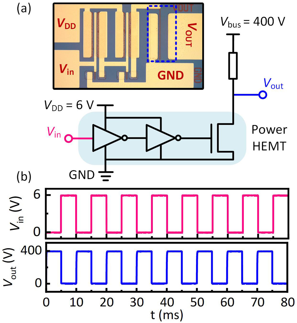
Figure 3: (a) GaN complementary logic buffers monolithically integrated with power HEMT driving external load resistor. (b) Input and output waveforms.
The complementary logic buffers operated at 6V VDD, typical for power ICs (Figure 3). The buffer was used to drive a 17μm gate-length power HEMT with a +1.3V E-mode threshold. The bus voltage of the HEMT was 400V.
The team comments: “The decent switching operation validates the capability of GaN complementary logic circuits for GaN power integrated circuits (PICs). As a preliminary study in university laboratory, the gate width of the power HEMT is only 100μm. To demonstrate fast-switching operation, a large-area power HEMT is required to minimized the influence of parasitic capacitances, which remains a future work.”
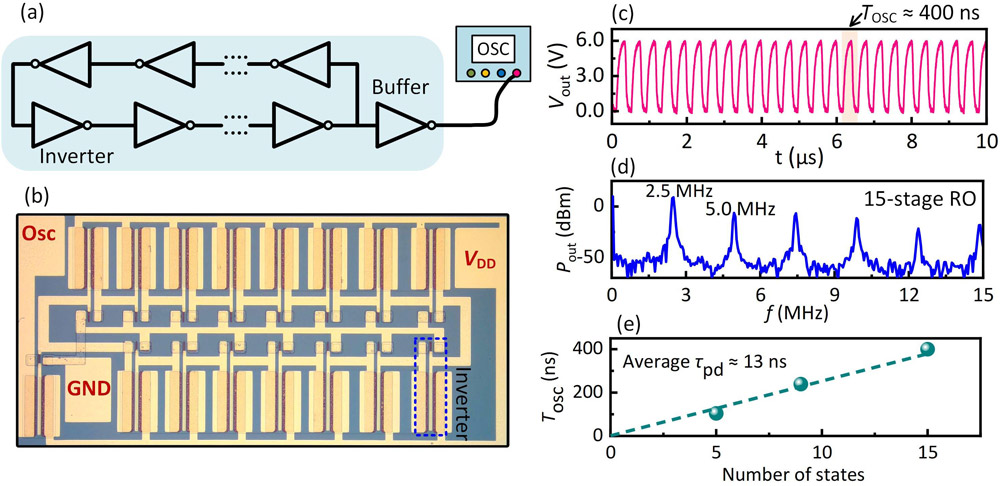
Figure 4: (a) Ring oscillator (RO) circuit. (b) Microscopic photograph of 15-stage RO. (c)–(d) Voltage waveforms and power spectrum of 15-stage RO at VDD = 6V, delivering ~400ns oscillating period (Tosc) and 2.5MHz fundamental frequency (fosc). (e) Tosc versus number of RO stages (N).
For the RO circuits (Figure 4), the researchers comment: “The GaN ROs in this work exhibit a breakthrough propagation delay τpd as short as ~13ns, compared with >30 ns in prior publications.”
https://iedm24.mapyourshow.com
The author Mike Cooke is a freelance technology journalist who has worked in the semiconductor and advanced technology sectors since 1997.


