News: Microelectronics
14 January 2025
High-breakdown-voltage P-GaN gate HEMTs with threshold voltage of 7.1V
Shandong University has reported an enhancement-mode P-GaN/AlGaN/GaN metal-insulator-semiconductor high-electron-mobility transistors (MIS-HEMTs) by combining thermal oxidation treatment of P-GaN with atomic layer deposition (OTALD) prior to gate metal deposition [Siheng Chen et al, IEEE Electron Device Letters, vol. 45, no. 12, pp2343–2346, December 2024, doi: 10.1109/LED.2024.3478819]. Compared with traditional devices, the device presented increased threshold voltage significantly from 1.8V to 7.1V, with improved gate breakdown voltage and off-state breakdown voltage of 26.9V and 1980V, respectively.
When used as power devices, P-GaN/AlGaN/GaN HEMTs require high threshold voltage, high gate voltage swing, high breakdown voltage and low gate leakage current. A low activation rate of magnesium (Mg) dopants in P-GaN typically results in a threshold voltage of less than 2V without additional processing, limiting the application of P-GaN/AlGaN/GaN HEMTs in high-gate-voltage drive circuits. Therefore, improving the threshold voltage is a pressing challenge. In response to this issue, the researchers applied a combination of oxygen annealing treatment (OT) of P-GaN and atomic layer deposition (ALD) technology, achieving the highest threshold voltage on record with high gate breakdown voltage and high off-state breakdown voltage. This research demonstrates the immense potential of OTALD technology in power electronic devices requiring high gate drive voltages, thereby expanding the possibilities for widespread application in P-GaN power devices.

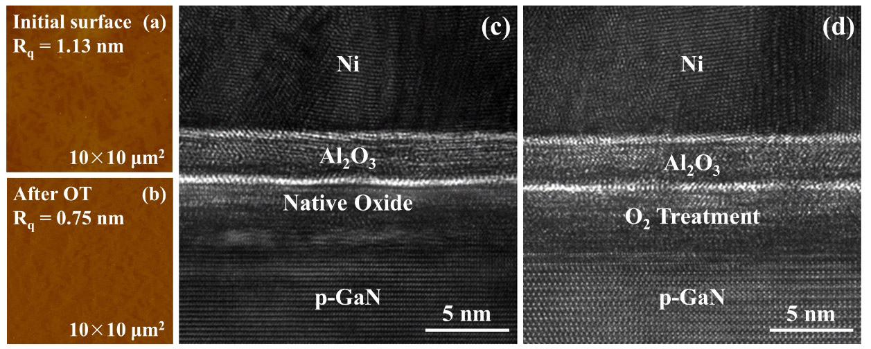
Figure 1: AFM-measured P-GaN surface profiles (a) before and (b) after OT process. Cross-sectional TEM image of the MIS contact of (c) ALD-HEMTs and (d) OTALD-HEMTs.
The epitaxial structure in this study based on a Si (111) substrate consists of a 100nm P-GaN cap layer with an Mg doping concentration of 3x1019cm-3, a 12.5nm Al0.18Ga0.82N barrier layer, a 0.5nm AlN spacer layer, a 450nm undoped GaN channel layer and a 4μm high-resistance GaN buffer layer that were grown by metal-organic chemical vapor deposition (MOCVD). Device fabrication commences with highly selective etching of the P-GaN cap layer, and mesa isolation of the device was completed subsequently by inductively coupled plasma (ICP) etching. The ohmic contacts were formed using a metal stack of Ti/Al/Ni/Au via magnetron sputtering and annealing in N2 atmosphere. After depositing a SiO2 passivation layer using plasma-enhanced chemical vapor deposition (PECVD), the opening of the gate region was patterned by ICP etching. The fabrication of the MIS structure on the opening of the P-GaN gate region by OTALD technology started with the thermal oxidation treatment. This is to form a thin oxide layer by low-temperature annealing process in oxygen atmosphere. Followed by deposition of a 5nm Al2O3 dielectric layer by plasma-enhanced atomic layer deposition (PEALD) process. Finally, a Ni/Au gate metal stack was deposited by magnetron sputtering to form the gate metal field plate. The untreated fresh P-GaN gate HEMTs were fabricated as references. All devices have the same size with a P-GaN gate length (LG) of 4μm, a gate–drain spacing (LGD) of 12μm, a gate–source spacing (LGS) of 4μm and a gate width (WG) of 100μm. The length of the gate field-plate is 2µm.
Atomic force microscopy (AFM) measurement shows decreased surface roughness after the oxygen annealing treatment process, indicating that this process produces a flat oxide layer on the P-GaN surface and effectively removes other contaminants. Cross-sectional high-resolution transmission electron microscopy (HRTEM) shows that a dense and smooth oxide layer is formed. The presence of this oxide layer provides a gradually varied transition between Al2O3 and P-GaN, leading to a significantly improved interface quality between these two materials.

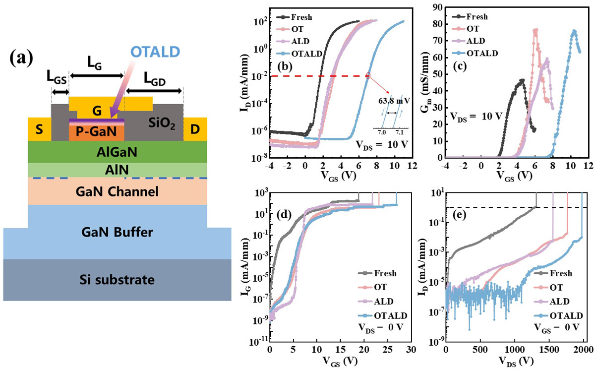
Figure 2: (a) Schematic cross section of OTALD-HEMTs. (b) Transfer and (c) transconductance characteristic of four types of P-GaN gate HEMTs. (d) Gate breakdown and (e) off-state breakdown characteristics of four types of P-GaN gate HEMTs.

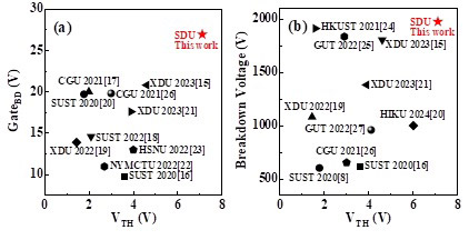
Figure 3: Comparison for (a) gate breakdown and (b) off-state breakdown with different threshold voltage between this work and other studies.
Owing to the higher gate Schottky barrier of the oxide layer and the voltage division effect of the dielectric layer, OTALD-HEMTs allow the threshold voltage to be increased significantly from 1.8V to 7.1V compared with conventional P-GaN gate HEMTs, with a minimal hysteresis of 63.8mV and high on/off current ratio above 108. The smooth interface of the oxide layer can reduce the scattering of the two-dimensional electron gas (2DEG) within the channel, contributing to a higher transconductance (75.9mS/mm, an increase of 63%) with a higher saturation output current density at VGS = 11V. The dense oxide layer possesses a wider bandgap and higher thermodynamic stability than P-GaN, which is less susceptible to degradation caused by hot-electron bombardment and suppression of gate leakage current. Also, the presence of the dielectric layer beneath the gate can reduce surface states and fill defects on P-GaN surfaces, decreasing the leakage current and suppressing hot-carrier effects. Thus, the OTALD-HEMT further enhanced the forward gate breakdown and off-state breakdown voltage to 26.9V and 1980V, which are improvements of 42% and 51% respectively compared with the conventional P-GaN gate HEMT. The OTALD-HEMTs exhibit the high gate breakdown voltage, off-state breakdown voltage as well as record highest threshold voltage among previously reported P-GaN gate devices, indicating that OTALD technology holds substantial potential for enhancing VTH and further improving device performance


