


News: Optoelectronics
20 March 2025
Indium arsenide quantum dot VCSELs on InP(311)B substrate
Sony Semiconductor Solutions Corp and Japan’s National Institute of Information and Communications Technology (NICT) claim the first demonstration of electrically pumped laser oscillation of C-band indium arsenide (InAs) quantum dot (QD) vertical-cavity surface-emitting lasers (QD VCSELs), fabricated on indium phosphide (331)B (InP(311)B) substrates by applying a strain compensation technique [Michinori Shiomi et al, Optics Express, v33, p12982, 2025].
The conventional C-band optical communication wavelength range is 1530–1565nm. The researchers see enhanced speed, reduced power consumption, and the feasibility for two-dimensional integration as key advantages of the VCSEL format over edge-emitting devices. Apart from communications, such properties are sought for 3D sensing dot projectors with high permissible exposure levels in the eye-safe short-wavelength infrared (SWIR) range greater than 1.4μm.
The team comments: “Achieving electrically pumped oscillation of QD VCSELs with InAs QD active layers on InP substrates could significantly enhance wavelength-division multiplexing communication, leveraging low-loss optical fibers around 1550nm.”
The researchers grew samples on InP(311)B substrates, using solid-source molecular beam epitaxy (Figure 1). Indium gallium aluminium arsenide (InGaAlAs) spacers between the QD layers provided strain compensation, enhancing crystallinity and maximizing QD density (~8x10¹⁰/cm2).
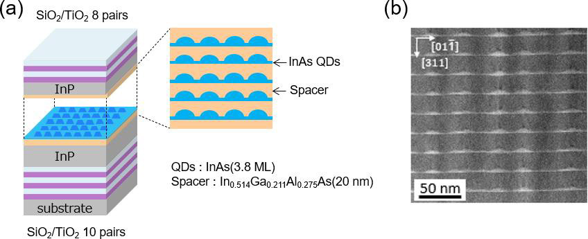
Figure 1: (a) Schematic of optically pumped QD VCSEL. (b) Cross-sectional HAADF-STEM image.
In optical pumping experiments, material with 5 QD layers achieved a full width at half maximum of 100nm and a design wavelength of 1550nm. The laser threshold pump power was 45μW, compared with 60μW for a InGaAsP quantum well (QW) VCSEL.
The researchers comment: “The lower threshold of the QD VCSEL compared to the QW VCSEL can be attributed to two factors: the smaller volume of the QD structure, which results in lower losses, and the δ-function-like density of states of QDs.”
The optical confinement was provided by silicon dioxide/titanium dioxide (SiO2/TiO2) layer pairs in dielectric distributed Bragg reflector (DBR) mirrors that put the QDs at an antinode of the electric field.
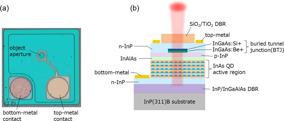
Figure 2: (a) Top-view and (b) cross-sectional schematic of electrically pumped QD VCSEL.
The material structure was modified to enable electrical pumping (Figure 2). The bottom dielectric DBR was replaced with 62 InP/InGaAlAs semiconductor layer pairs. Also, an InGaAs tunnel junction with silicon (Si) and beryllium (Be) doping was implemented for hole injection into the InAs QD region. The aperture diameter was 12μm.
The peak output power was 0.17mW at 25mA pulsed injection (Figure 3). The threshold was 13mA. “The observed nonlinearity in the light–current (L–I) curve is attributed to the rollover phenomenon, which is caused by the carrier overflow under thermal effects under bias conditions,” the team comments. The laser wavelength at 15mA was 1536nm. The researchers say that tuning to the 1550nm wavelengths favored by optical communications could be provided by adjusting the cavity length.
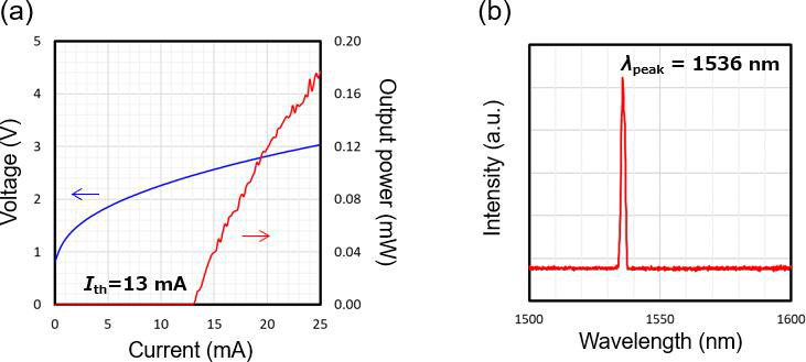
Figure 3: (a) Light output power and voltage versus current characteristics of QD VCSEL. (b) Spectrum at 15mA.
Optical polarization measurements showed alignment with the InP[−233] direction. The InP crystal structure also affected the QD shape, giving an elliptical form with 33.0nm major axis along the InP[−233] direction and 19.8nm minor axis along the InP[01−1] direction, according to plan-view high-angle annular dark-field scanning transmission electron microscopy (HAADF-STEM) images.
The team comments: “The emission characteristics of elliptical QDs are typically polarized along their major axis due to inherent shape effects, and the findings of this study are in agreement with this behavior. However, the previously reported strain induced during crystal growth may also influence polarization control, implying that the observed polarization behavior is influenced by a combination of both shape and strain effects.”
Good optical polarization control could open up a range of applications, which cannot be provided easily in QW VCSELs.
The team hopes that further work will enable communication applications requiring 1mA thresholds and 1mW output power at higher temperatures and under high-speed direct modulation.
https://doi.org/10.1364/OE.551300
The author Mike Cooke is a freelance technology journalist who has worked in the semiconductor and advanced technology sectors since 1997.


