


News: Optoelectronics
25 March 2025
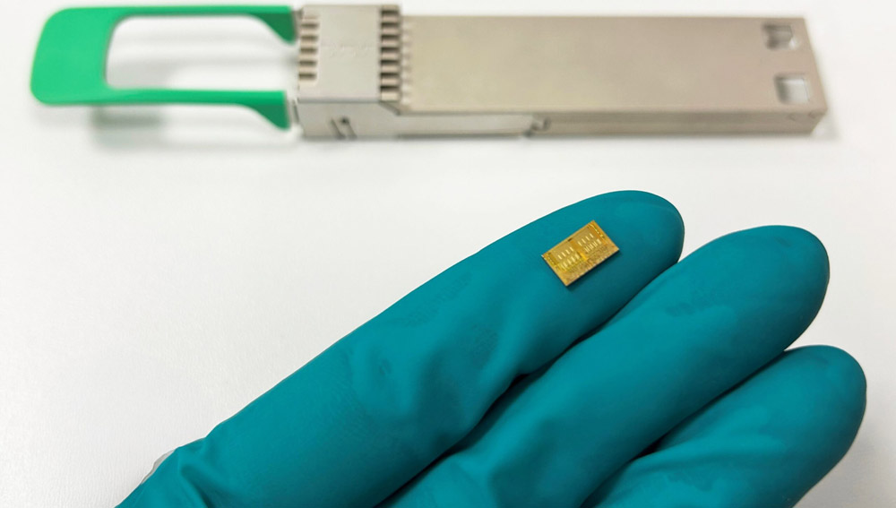
Scintil demonstrating LEAF Light DWDM remote light source at OFC
In booth 6357 at the Optical Fiber Communications Conference & Exposition (OFC 2025) in San Francisco, CA, USA (1–3 April), Scintil Photonics of Grenoble, France (a fabless firm developing and commercializing silicon photonic integrated circuits with integrated lasers for AI data centers) is demonstrating LEAF Light, which is claimed to be the world’s first single-chip, multi-wavelength laser source that delivers the speed, reach, power efficiency and lower latency required for scale-up networks. Scintil’s compact dense wavelength division multiplexing (DWDM) remote light source (with what is claimed to be the world’s most precise wavelength spacing) is said to be a vital component within the emerging co-packaged DWDM architecture that addresses the challenges for scalable AI data centers.
As copper cables hit their limit in speed and reach for AI interconnects, DWDM co-packaged optics is emerging as the ultimate optical networking solution for AI data centers, says Scintil. Compared with legacy coarse wavelength division multiplexing (CWDM) implementation, DWDM will reduce latency, boost power efficiency, increase bandwidth density and enable up to 2 terabits per second (Tbps) in a single fiber.
“LEAF Light is the only single-chip solution that can meet all the system requirements at an acceptable size and cost for the emerging co-packaged DWDM architecture that requires the finest, high-precision multi-wavelength light source to efficiently transmit data,” claims CEO Matt Crowley. “Our aim is to closely align volumes of LEAF Light with the growth in the XPU accelerator market, expected to reach $600bn in 2030 with about 35 million AI accelerators,” he adds. “We are sampling a limited number of select customers later this year, with broader availability of our External Laser Small Form-Factor Pluggable (ELSFP) engineering samples in 2026.”
LEAF Light is manufactured using Scintil’s proprietary SHIP (Scintil Heterogeneous Integrated Photonics) process technology. This silicon photonics process integrates III–V and other materials into the standard silicon photonics process flows now available from commercial foundries. The firm says that the process compatibility with standard silicon photonics fabs and wafer-scale manufacturing gives LEAF Light the capability to scale to tens of millions of units per year and beyond.
“In close collaboration with customers, we have developed a single-chip light source solution, featuring 8–16 multiplexed lasers with 200GHz or 100GHz frequency spacing, respectively,” notes Sylvie Menezo, founder & chief technology officer. “In addition, we have developed the control electronics and the optical packaging to fit into an ELSFP.”
Sylvie Menezo has been invited to discuss light sources for co-packaged optics switches and XPU systems in the following presentation at OFC’s Technical Conference:
- ‘High Power and Multi-Wavelength Laser Light Sources: How Can They Address the Needs of AI/ML Interconnects’ Workshop (30 March, 13:00–15:30 PDT);
- ‘Advanced Packaging and Integrated Optics for Scale-Up AI Interconnects’ Symposium (2 April, 14:00–18:30 PDT).
Scintil appoints Matt Crowley as CEO and establishes US subsidiary


