


News: LEDs
13 March 2025
Full-color monolithic micro-LED displays
Japan-based Toyoda Gosei Co Ltd reports progress towards full-color monolithic micro-light-emitting diode (LED) display based on stacked indium gallium nitride (InGaN) layers aimed at red-green-blue (RGB) emission [Koichi Goshonoo et al, Appl. Phys. Express, v18, p022003, 2025].
The researchers comment: “The proposed semiconductor process-based method enables the fabrication of low-cost and high-resolution micro-displays.”
Although the regrowth steps used can be seen as increasing process complexity and costs, the team argues “other methods that do not require regrowth, combining blue monolithic micro-LEDs with quantum dots requires materials and equipment different from conventional semiconductor processes, and stacking RGB epitaxial layers via tunnel junctions needs complex driving circuits.”
The micro-display market is growing with gradual performance enhancements hopefully expanding applications beyond virtual reality goggles and electronic view-finders. To allow use in sunlight, such as for augmented reality glasses, higher-brightness displays are needed. Presently, commercial micro-displays are organic LED based, but higher brightness would probably be better delivered by monolithic InGaN micro-LEDs.
The material for the micro-display chips was grown by metal-organic chemical vapor deposition (MOCVD) on patterned sapphire (Figure 1). The p-type electrodes for the separate RGB layers were applied in a regrowth step after selective removal of the material grown in the initial MOCVD.
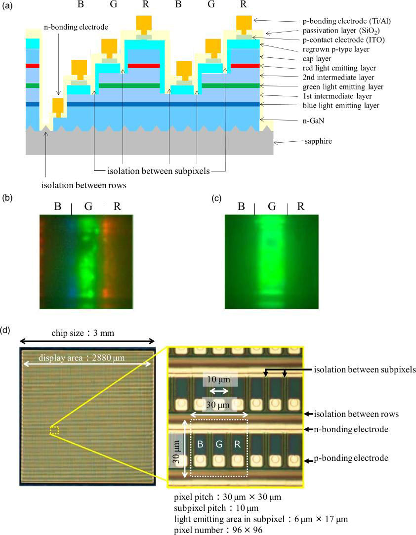
Figure 1: (a) Cross-sectional structure of full-color monolithic micro-LED. (b) Electroluminescence (EL) image of sub-pixels without inter-sub-pixel isolation. (c) EL image of sub-pixels with inter-sub-pixel isolation. (d) Photograph of fabricated monolithic micro-LED chip.
Further fabrication involved mesa isolation, indium tin oxide (ITO) p-electrode deposition and isolation, silicon dioxide (SiO2) passivation, and n- and p-metal bond pads.
The team reports that it has added two additional dry-etch steps over its previous micro-display work: “removing n-GaN and isolating each row for passive matrix driving and removing the p-type layer between adjacent sub-pixels.” Without the p-electrode isolation, the devices suffered from unintended emissions between adjacent sub-pixels.
The researchers comment: “Each row in a passive matrix circuit is connected to a common cathode, eliminating the need to remove the n-GaN between adjacent sub-pixels within the same row to isolate them; only the p-type layer is removed. However, the n-GaN between the rows needs to be removed for the passive matrix circuit to function correctly.”
The completed chips consisted of a 96x96 pixel array with a 2.88mmx2.88mm total display area. The chip itself measured 3mmx3mm.
Under probing experiments (Figure 2), the team found wavelength shifts of 21nm, 23nm and 8nm, respectively, for the RGB sub-pixels, between 20μA and 200μA current injection. The drive voltages were around 0.7V lower for R pixels against the GB pixels, explainable by the narrower 2.1eV bandgap for the R active material versus 2.7eV for B. The G pixel’s drive voltage was around or even higher than that for B, “which is presumed to be due to the process of forming the multi-color structure,” the researchers explain.
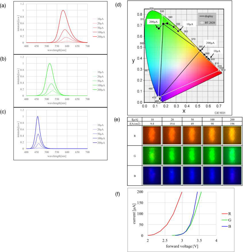
Figure 2: (a)–(c) EL spectra of red, green and blue sub-pixels, respectively, over 10–200μA current range. (d) Chromaticity diagram. (e) EL images. (f) Current–voltage characteristics for each sub-pixel color.
Indirect estimates for the external quantum efficiencies (EQEs) are given as 0.2%, 2% and 3% for the RGB pixels, based on comparison with regular-size LEDs. Direct assessment is hampered by the difficulty posed by micro-emission measurements.
The researchers comment: “The efficiency of red is one order of magnitude lower than the other colors due to the difficulty of InGaN red emission, and the efficiency of green and blue is also lower than the monochromatic ones due to the process specific to the structure considered in this study.”
The team also reports: “The resulting color gamut covered 57.6% of ITU-R Recommendation BT.2020 (BT.2020) and 69.9% of the National Television System Committee (NTSC) standard.” The gamut was much narrower than the group’s previous work achieving 95.4% NTSC coverage. “This reduction is primarily attributed to a shorter red-emission wavelength, resulting from both the quality of the red-light-emitting layer and high current injection,” the researchers write, adding: “This limitation can be addressed by adjusting the red-light-emitting layer.”
The chips were wired up in a passive-matrix format and connected to a driver circuit that included a Teensy 4.1 microcontroller, which generated the serial data and clock signals. The data were converted into parallel format to drive the individual pixels via shift-register circuits and transistor arrays.
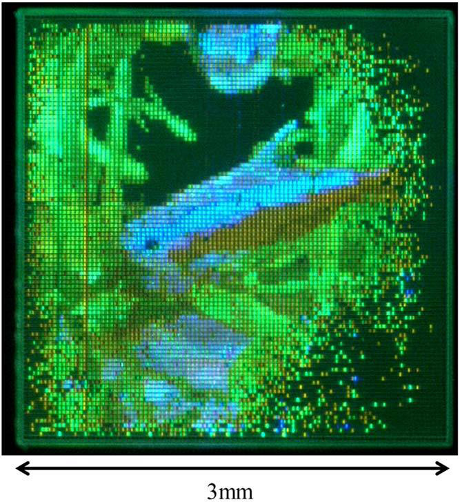
Figure 3: Display image of monolithic micro-LED array.
The team rendered a 4-bit grayscale RGB image via pulse-width modulation (PWM) of a cardinal tetra fish (Figure 3). The blue/red color of this species in the image suffered from the low quality of the red channel. This could possibly be corrected with more precise current and/or pulse-width adjustments to compensate for the lower R pixel efficiency performance.
There were also non-emitting regions in the periphery of the chip, due apparently to insufficient bonding pressure during the chip-to-submount bonding process.
Full-color monolithic micro-LEDs InGaN Sapphire substrates MOCVD
https://doi.org/10.35848/1882-0786/adb5ec
https://en.wikipedia.org/wiki/Cardinal_tetra
The author Mike Cooke is a freelance technology journalist who has worked in the semiconductor and advanced technology sectors since 1997.


