


News: LEDs
6 March 2025
Aluminium nitride template strategies for brighter UVC LEDs
Researchers based in China have been exploring strategies to improve deep ultraviolet (UVC, 100–280nm) light-emitting diode (LED) performance on sapphire, focusing on the aluminium nitride template layers used as a base for the aluminium gallium nitride (AlGaN) device materials [Xu Liu et al, IEEE Transactions On Electron Devices, published online 11 February 2025].
Their work achieved a 71% increase in external quantum efficiency (EQE), compared with a UVC LED grown on epitaxial layer overgrowth (ELO) AlN/sapphire. The researchers also report that the EQE of the 272nm-wavelength LED was almost 90% greater than that of a device on a conventional AlN buffer template. Short-wavelength UVC kills pathogens by disrupting the biochemical structures, such as DNA and RNA, vital to life.
The team from Wuhan University, Wuhan Joint Innovation Laboratory of Advanced Display Industry, and Ningbo ANN Semiconductor Company Ltd., report: “Using nanolayer modification, growth-mode modulation, and indium-doping methods, the crack-free, strain-controlled, and atomically smooth AlN buffer template was achieved on the sapphire substrate.”
The researchers see their work as promising for improved sustainability and environmentally friendly germicidal irradiation sources.
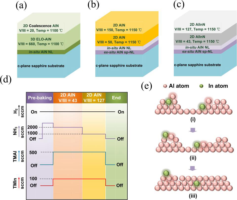
Figure 1: Epitaxial structure of (a) AlN-I, (b) AlN-II and (c) AlN-III. Schematic illustrations of (d) growth conditions of AlN-III and (e) underlying mechanism of indium modulation.
The researchers compared three strategies (Figure 1) for creating AlN buffer templates on 2-inch flat sapphire substrate (FSS) by metal-organic chemical vapor deposition (MOCVD).
The first method (AlN-I) used a 1.33μm epitaxial layer overgrowth process with a three-dimensional (3D) mechanism to reduce defects in subsequent material growth layers. The 2D coalescence layer was 1.85μm. The initial nucleation for the epitaxial crystal growth was carried out in-situ by MOCVD.
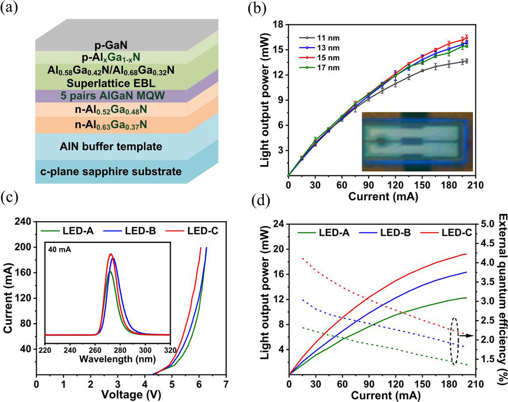
Figure 2: (a) Schematic of UVC LED with superlattice electron-blocking layer (EBL). (b) Light output power versus current injection on AlN-II buffer templates with varied thickness ex-situ AlN sp-NL. Inset: microscope image of lit UVC LED. (c) Current–voltage characteristics of LED-A, -B and -C. Inset: EL spectra at 40mA. (d) Light output power/EQE-current characteristics.
The other two methods (AlN-II/III) prepared the FSS with a 12nm ex-situ sputtered nucleation layer (sp-NL). The sp-NL was annealed at high temperature after deposition to clean the surface and help improve the structure through lattice rearrangement. The optimum thickness of the sp-NL was found to be 15nm (Figure 2).
On transfer to the MOCVD chamber, the growth continued with an in-situ NL, and then two 2D growth steps with different V/III ratios at a higher 1150°C temperature, compared with 1100°C for AlN-I.
AlN-II and AlN-III differed in the V/III ratios, and in AlN-III included indium in its composition: the trimethyl-Al/-In precursors were supplied in the flux ratio 5:1.
The researchers explain the underlying mechanism of the indium modulation of AlN-III: “The In–N bond energy is much weaker than Al–N bond energy. This will lead to the lower activation barrier of indium diffusion than that of aluminium diffusion on the AlN film so that indium adatoms tend to wander freely on the AlN rather than aggregate to form clusters. When diffused indium atoms contact with the step edge of an AlN grain island, it can reduce the Ehrlich–Schwoebel barrier for aluminium atoms to descend steps, as shown in processes (i) and (ii), which is beneficial for the 2D growth of AlN epitaxial film.”
The weakness of the In–N bond also means that, once it moves, the vacancy is preferably filled with aluminium, leading to a smoother AlN film. When on the relatively rare occasion that an indium atom is incorporated, it also acts to relieve the strain from the AlN/sapphire lattice mismatch: InN has a larger lattice constant than AlN.
With a view to subsequent AlGaN growth on the AlN templates, the team comments: “Generally, the AlGaN upper layer grown on the AlN film is anticipated to undergo severe compressive strain due to the large mismatch at the interface between AlN and AlGaN. This will impair the crystalline quality, roughen the surface, and weaken the overlap of electron–hole pairs in the active region, thereby undermining the emission performances of UVC LEDs.”
The indium modulation stretches the AlN lattice, suppressing the mismatch between AlGaN and the template. The AlN/sapphire templates were used to grow AlGaN UVC material and fabricate 0.254mmx0.508mm LEDs.
Atomic force microscopy on a 10μmx10μm field showed root-mean-square roughness values of 6.69nm, 1.21nm and 0.49nm for AlN-I, -II and -III, respectively. In 2μmx2μm regions clear of stack faults and hillocks, the corresponding roughnesses were as low as 1.63nm, 0.34nm and 0.24nm, respectively. Dislocation densities based on x-ray diffraction analysis were estimated at 5.1x10⁹/cm2, 2.8x10⁹/cm2 and 1.5x10⁹/cm2 for the samples AlN-I, -II and -III, respectively.
The researchers comment: “The lowest dislocation density was achieved in AlN-III, indicating that indium atoms were well incorporated into the lattice of the AlN epitaxial film, thereby avoiding the generation of dislocations or parasitic crystal grains owing to the localized agglomeration of InN phase from degrading the crystalline quality of AlN epitaxial film.”
The LEDs-A, -B and -C, based on templates I, II and III, respectively, showed much improved performance for C over A and B (Figure 2).
Table 1: Measured forward voltage (VF), light output power (LOP), and external quantum efficiency (EQE) for LEDs-A, -B and -C.
LED |
VF @ 200mA | LOP @ 200mA | peak EQE |
| A | 6.28V | 12.5mW | 2.4% |
| B | 6.27V | 16.3mW | 3.0% |
| C | 6.07V | 19.1mW | 4.1% |
In particular, LED-C showed reduced forward voltage, and increased light output power and efficiency (Table c). Reduced VF indicates that the device is consuming less power for a given current injection, boosting efficiency. The peak EQE was achieved around 15mA injection. The peak wavelength was 272nm.
https://doi.org/10.1109/TED.2025.3538815
The author Mike Cooke is a freelance technology journalist who has worked in the semiconductor and advanced technology sectors since 1997.


