


News: Microelectronics
22 May 2025
High-breakdown normally-off gallium oxide transistors
Saudi Arabia’s King Abdullah University of Science and Technology (KAUST) has claimed record breakdown voltages for normally-off beta-phase gallium oxide (β-Ga2O3) metal-oxide field-effect transistors (MOSFETs) on gallium nitride (GaN) on silicon substrate [Mritunjay Kumar et al, Appl. Phys. Lett., p126, p193505, 2025].
The reported maximum reverse-bias breakdown was measured at 540V, the highest among previously reported studies on breakdown voltage of β-Ga2O3 MOSFETs on silicon substrates, according to the KAUST team. The β-Ga2O3 material is presently in the laboratory phase of its device development, and the ultimate breakdown capability enabled by the 4.9eV ultrawide bandgap is presumably some way off. This bandgap should be able to sustain electric fields up to 8MV/cm. Commercial advanced power handling materials include GaN and silicon carbide (SiC) with wide bandgaps up to 3.4eV.
The researchers comment: “Despite advancements in β-Ga2O3 thin-film growth technology via various growth methods on heterogeneous substrates, there is no demonstration of β-Ga2O3 power MOSFETs utilizing GaN buffer-on-Si substrates.”
The use of low-cost, commercially available GaN/Si substrates is seen as being “significant for high performance and their monolithic integration with GaN devices in future power integrated circuits”. In particular, more thermally conductive GaN on Si could ease the temperature management problems of β-Ga2O3. Other options for thermally conductive substrates include SiC, but these substrates are very costly.
In addition to power handling, the KAUST team suggests that the combination with GaN could enable β-Ga2O3 radio frequency devices for power switching and RF amplification systems.
The researchers explain: “Given β-Ga2O3’s higher breakdown voltage compared to GaN, it complements GaN’s superior mobility. This allows high-speed control circuitry to be implemented with GaN technology, while high-power devices are realized using β-Ga2O3, leveraging both technologies to develop monolithic power-integrated circuits (ICs).”
The researchers used an economical and scalable β-Ga2O3 growth technique: pulsed laser deposition (PLD).
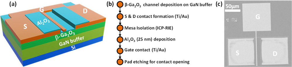
Figure 1: β-Ga2O3 TFT device structure: (a) three-dimensional (3D) schematic, (b) process flow, (c) scanning electron microscope (SEM) image.
TFTs (Figure 1) were fabricated on 50nm β-Ga2O3 layers on 4.7μm GaN on p-Si(111) substrates. The β-Ga2O3 was doped with silicon to give an n-type electron majority carrier character. The semi-insulating GaN buffer contained a carbon doping concentration of 5x10¹⁹/cm3.
The β-Ga2O3 layers were grown by 700°C PLD with a 102mJ/pulse laser ablating Ga at 5Hz in an environment with oxygen at 5mTorr partial pressure. The electron transport properties gave 1.2x10¹⁸/cm3 electron concentration and 2.06cm2/V-s mobility from Hall-effect measurements.
The researchers comment: “The relatively low bulk mobility of the epitaxial β-Ga2O3 film is primarily due to its polycrystalline nature, and lattice-mismatch-induced defects from growth on GaN/Si substrates.”
The team suggest that mobility could be enhanced by deploying metal-organic chemical vapor deposition (MOCVD) growth rather than PLD. With post-deposition annealing this would increase crystallinity and decrease defect density.
The surface roughness of the β-Ga2O3 was 0.57nm, doubling the 0.23nm of the underlying GaN substrate, according to atomic force microscopy (AFM) on a 5μmx5μm field.
The source/drain (S/D) electrodes of the TFTs consisted of titanium/gold (Ti/Au). The gate (G) structure consisted of 25nm aluminium oxide (Al2O3) dielectric and Ti/Au electrodes. The gate length (Lg) was 4μm; and, the S (LSG) and D (LGD) distances to the gate were 3μm and 18μm, respectively.
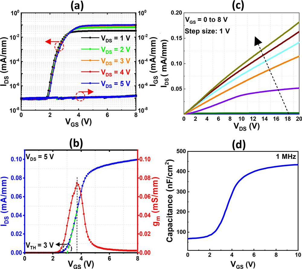
Figure 2: Electrical characteristics: (a) current-gate voltage transfer (IDS–VGS) at different VDS, (b) VTH calculation by linear extrapolation at transconductance (gm) maximum, (c) output characteristics at different VGS, (d) capacitance–voltage (C–V) measurement at 1MHz.
The TFTs demonstrated a low 167mV/decade subthreshold swing (SS) and high 106 on/off current ratio (Figure 2). The team comments: “The low SS for the fabricated device indicates a high-quality interface between β-Ga2O3 and Al2O3.”
The interface trap density (Dit) was estimated to be 4x10¹²/cm2-eV, using capacitance–voltage measurements.
The Al2O3 dielectric enabled a small gate leakage of order 10−7mA/mm at 8V forward gate potential. The transistor threshold was at +3V at 5V VDS, giving enhancement-mode (normally-off) behavior. Such behavior is favored for fail-safe power system operation.
The researchers comment: “The positive VTH of β-Ga2O3 MOSFETs is contributed by both the top-side and bottom-side depletion, along with possible phase-induced insulating regions near the β-Ga2O3/GaN interface.”
The team reports that the threshold point can be controlled by the β-Ga2O3 layer thickness.
A field-effect mobility of 1cm2/V-s was extracted from transconductance measurement, using a transistor with a 30μm-long, 150μm-wide gate at 0.1V drain bias. The maximum drain current was 0.18mA/mm at 8V gate potential, and 20V drain bias. The on-resistance (Ron) was estimated to be 13.6kΩ-mm in the linear region.
Table 1: Electrical parameter comparison of reported β-Ga2O3 TFTs on heterogeneous substrate. KAUST work in bold.
Material preparation method |
Substrate | VTH (V)/operation mode | Ron (kΩ-mm) | Ion/Ioff | Vbr (V) |
| MOCVD | Sapphire | D-mode | >107 | 390 | |
| MOCVD | Sapphire | D-mode | 1011 | 400 | |
| MOCVD | AlN/Si | −2.17 | 0.177 | 108 | 178 |
| **PLD** | **GaN/Si** | **3** | **13.6** | **106** | **540** |
| Exfoliation | SiO2/Si | −7.3 | >106 | 344 | |
| Exfoliation | SiO2/Si | 7 | 0.013 | 1010 | 185 |
| Ion-cutting | Al2O3/Si | D-mode | 3 | 106 | 522 |
| Ion-cutting | Al2O3/SiC | D-mode | 0.101 | 107 | 1000 |
| Fusion bonding | β-Ga2O3/4H-SiC | −50 | 0.065 | 108 | 2000 |
The researchers also compare their work with other reported attempts to fabricate β-Ga2O3 TFTs on various heterogeneous substrates by various methods (Table 1).
GaO MOSFETs GaN Silicon substrate
https://doi.org/10.1063/5.0263220
The author Mike Cooke is a freelance technology journalist who has worked in the semiconductor and advanced technology sectors since 1997.


