


News: Optoelectronics
8 May 2025
Reducing thresholds for L-band quantum dot laser diodes
Researchers based in the UK and France claim the lowest threshold current per quantum dot (QD) layer reported for C-/L-band indium arsenide (InAs) QD lasers on (001) indium phosphide (InP) substrate [Jae-Seong Park et al, Optics Express, v33, p19158, 2025].
The team from University College London and Cardiff University in the UK and University Grenoble Alpes, France, report: “The fabricated seven-stack as-cleaved lasers (15μmx2000μm) under pulsed injection exhibit a record-low threshold current density (Jth) of 69A/cm2 per QD layer, surpassing previously reported values for C-/L-band InAs/InP QD lasers on (001) InP, and a maximum operating temperature of 130°C.”
The maximum temperature of 130°C is also claimed to be the highest so far for as-cleaved InAs/InP QD laser diodes on (001) InP. The neighboring conventional (C) and long-wavelength (L) optical fiber communication bands cover the ranges 1530–1565–1625nm, respectively.
The researchers comment: “The development of high-performance and reliable C-/L-band semiconductor lasers as light sources is of critical importance for optical communication systems due to the ever-growing data traffic demand, which has been further accelerated by recent advancements in artificial intelligence and machine learning applications.”
It is hoped that by using self-assembled QDs rather than quantum wells as an optical gain medium laser diodes with lower thresholds and better thermal stability can be fabricated. However, QD formation is somewhat inhibited due to the lower 3.2% lattice mismatch between InAs and InP, relatively to the 7.2% InAs mismatch to gallium arsenide (GaAs), suitable for ‘original’ (O)-band (1260–1360nm) laser diodes. The higher mismatch for the InAs/GaAs combination reduces the dot size dispersion, improving laser diode performance parameters.
The molecular beam epitaxy (MBE) structure for the laser diodes was grown on sulfur-doped n-InP substrate (Figure 1). The main waveguide layers consisted of lattice-matched indium aluminium gallium arsenide material: In0.524Al0.476As and In0.528Al0.238Ga0.234As, grown at 500°C and 485°C, respectively. On the bottom n-type side the material was doped with silicon (Si). For the p-type top layers, beryllium (Be) provided the doping.
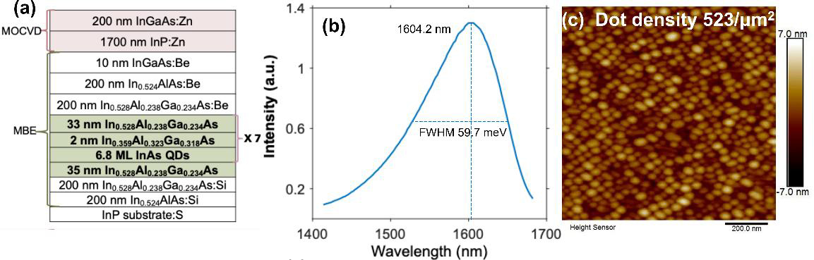
Figure 1: (a) Epitaxial scheme for InAs/InP QD laser. (b) Room-temperature (RT) photoluminescence (PL) spectrum of 7-layer InAs/InP QD laser material. (c) Atomic force microscopy (AFM) image of uncapped InAs/InP QDs.
The seven layers of quantum dots were grown on the InAlGaAs layers by first applying 6.8 monolayers (MLs) of InAs at 485°C. A 10s growth interruption under arsenic pressure enabled the QD formation with reduced size dispersion.
The QDs were first capped with 2nm strained In0.359Al0.323Ga0.318As, followed by temperature elevation to 515°C under arsenic over-pressure for 3 minutes. The second 33nm In0.528Al0.238Ga0.234As cap/spacer layer was then grown at 485°C.
The researchers comment: “This indium-flush technique ensures the high-quality stacking of the QDs by manipulating the morphology and the strain around the QDs.”
The MBE was completed with Be-doped InAlGaAs, InAlAs, and 10nm In0.532Ga0.468As. The final protection layer reduced oxidation during transfer to the metal-organic chemical vapor deposition (MOCVD) equipment, where the zinc (Zn)-doped InP cladding, and InGaAs contact layers were grown.
The researchers fabricated the material into Fabry–Pérot laser diodes with 15μm ridge width. The etched ridges were passivated with 400nm silicon dioxide (SiO2). The p-type electrodes consisted of titanium/gold. The n-metal contact was deposited on the backside of the wafer, consisting of nickel/gold-germanium/nickel/gold layers. The samples were annealed at 380°C to give ohmic contact at the metal/semiconductor interfaces. The laser cavity length was defined by cleaving. The facets were not coated.
The lowest threshold pulsed current density of 483A/cm2 was achieved from a laser diode with 2000μm cavity length. This translates to 69A/cm2 per QD layer. The researchers believe that the threshold could be further reduced with high-reflectivity facet coatings. This device continued operating as a laser up to 130°C, “the highest operation temperature reported so far for an as-cleaved InAs/InP QD laser on (001) InP”, according to the team. Facet coating, again, could increase this, as demonstrated by other reports of lasing above 130°C.
Shorter 1000μm- and 500μm-long laser diodes had a slightly lower maximum temperature of 120°C.
Table 1: Characteristic temperatures for threshold current (T0) and slope efficiency (T1).
Cavity length |
T0, T < 70°C | T0, T > 70°C | T1, T < 70°C | T1, T > 70°C |
| 500μm | 55.3K | 37.2K | 91.2K | 22.9K |
| 1000μm | 50.9K | 39.0K | 107.1K | 47.3K |
| 2000μm | 48.2K | 44.9K | 151.1K | 27.4 K |
The researchers calculated characteristic temperatures (Table 1) over the temperature ranges 20–70°C and 70–110°C. Higher characteristic temperatures indicate better thermal stability of the relevant parameters, threshold current and slope efficiency. The researchers mainly attribute the stronger degradation of T0 for shorter-cavity laser diodes at higher temperature to “increased mirror losses, which lead to higher carrier densities and thus increased non-radiative recombination, as well as reduced heat dissipation.”
The team comments: “At lower temperatures (20–70°C), longer-cavity devices exhibit higher T1 values due to lower mirror losses and reduced carrier leakage, leading to better slope efficiency retention. However, at higher temperatures (70–110°C), the longest cavity (2000μm) shows a noticeable degradation in T1, indicating a pronounced decline in slope efficiency. This is predominantly driven by thermally activated carrier escape from QDs, which is more detrimental in longer cavity lengths due to their inherently lower carrier density.”
The strong degradation of T1 for the 500μm laser diode is apparently related to “excessive mirror losses, which significantly increase carrier density and lead to enhanced non-radiative recombination.” The team adds: “This mechanism becomes a major contributor to T1 degradation in shorter cavities at high temperatures, contrasting with the thermal carrier escape that primarily affects longer cavities.”
The peak wavelengths at RT were 1624nm, 1613nm and 1592nm for 2000μm, 1000μm and 500μm cavity length, respectively (Figure 2). The blue-shift to shorter wavelengths in the shorter cavities is attributed to “increased threshold gain requirement due to higher mirror losses, which forces preferential lasing at shorter wavelengths where the QD ensemble provides higher gain”.
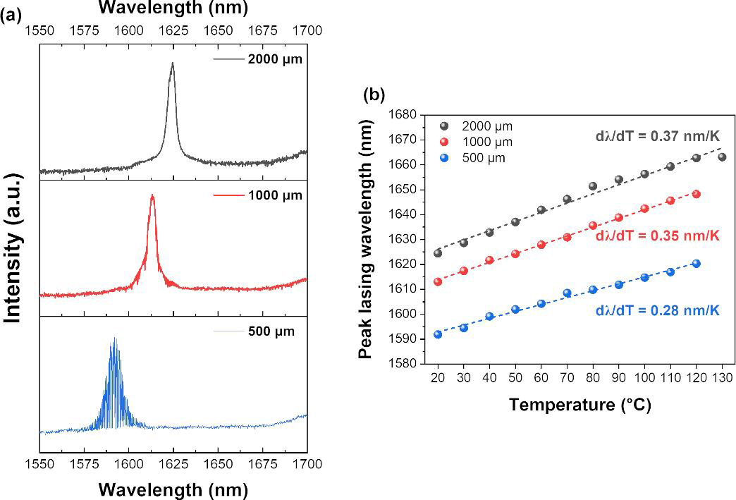
Figure 2: (a) RT lasing spectra at injection current of 1.1xIth and (b) temperature-dependent peak lasing wavelengths with cavity lengths of 2000μm, 1000μm and 500μm.
The researchers comment: “The reduced temperature sensitivity in shorter cavities can be ascribed to two factors: (i) suppressed mode hopping due to larger longitudinal mode spacing, which relatively stabilizes the wavelength shift, leaving only the dominant intrinsic red-shifts from bandgap shrinkage and temperature-induced refractive index change, and (ii) enhanced contribution of smaller QDs and/or higher-order transitions, driven by higher mirror losses that increase threshold gain requirements.”
The team also reports that a 3000μm-cavity laser diode achieved a threshold of 440A/cm2, or 63A/cm2 per QD layer, but at a cost of reducing the maximum operating temperature to 110°C, along with “evidence of mode hopping in the temperature-induced wavelength shift — namely, thermal and spectral instabilities”.
Some preliminary work on RT continuous-wave (CW) operation resulted in a threshold of 187.1A/cm2 per QD layer for 2000μm-cavity-length laser diodes. The peak wavelength shift was 0.76nm/K, and the maximum operating temperature 35°C.
InAs QD lasers InAs InP substrate MBE
https://doi.org/10.1364/OE.561471
The author Mike Cooke is a freelance technology journalist who has worked in the semiconductor and advanced technology sectors since 1997.


