


News: Microelectronics
2 May 2025
First post-process diamond on GaN HEMT
Stanford University and University of California Santa Barbara (UCSB) in the USA have claimed the first post-process diamond integration on a radio frequency (RF) gallium nitride (GaN) high-electron-mobility transistor (HEMT) [Rohith Soman et al, Appl. Phys. Express, v18, p046503, 2025]. The researchers see this as “a valuable platform for the thermal management of X-band GaN HEMTs using diamond heat spreaders.”
The team comments: “Self-heating causes the channel temperature to peak at the drain edge of the gate electrode, resulting in reduced channel mobility and shorter lifetime. This necessitates device-level cooling methods for reducing junction/channel temperature in RF power amplifiers, alongside conventional package-level cooling techniques.”
The X-band covers frequencies in the range 7–12GHz with applications in communications and radar. GaN HEMTs can suffer from performance degradation and poor reliability when temperatures increase due to insufficient heat dissipation of the high input power. It is hoped that high-thermal-conductivity diamond can be used to transmit the heat away from the device structure.
The researchers report: “We integrated diamond on the top and sidewalls of the device active area. The top-side heat extraction method provides an alternate path for heat dissipation through the deposited diamond bypassing the high resistance of the buffer/nucleation layers in the growth stack. Additionally, N-polar devices have an AlGaN barrier layer placed below the GaN channel layer; hence the top diamond is within 10nm of the hot spot and can be extremely efficient.
GaN RF device development is particularly targeted at high power density to enable longer transmission distances and better signal quality with low noise.
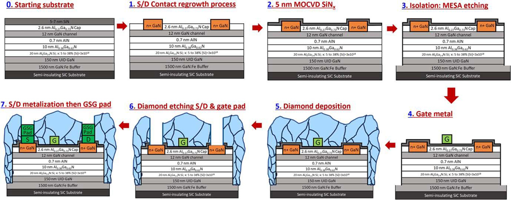
Figure 1: Sequence of steps followed in fabrication of all-around diamond integrated N-polar GaN HEMT device with ‘device first’ approach.
The GaN HEMT with an aluminium gallium nitride (AlGaN) barrier, and in-situ silicon nitride (SiN), structure (Figure 1) was grown on 2-inch semi-insulating silicon carbide (SiC) substrate by metal-organic chemical vapor deposition (MOCVD). The researchers used a N-polar rather than Ga-polar III–nitride structure, since such materials result in enhanced power densities, two-dimensional electron gas (2DEG) profiles, and scaling performance.
Before the diamond deposition, a metal-insulator-semiconductor (MIS)HEMT was fabricated with MOCVD regrown heavily doped n+-GaN source/drain contacts, MOCVD SiNx gate dielectric, and molybdenum (Mo) gate electrode. The individual devices were electrically isolated by mesa etching. The device was capped with an atomic layer deposition (ALD) silicon dioxide (SiO2) protection layer for the diamond deposition process. The source/drain distance was 1μm (LSD), the gate was 150nm long (LG), and the gate–drain spacing was 400nm (LGD).
The all-around diamond covered the whole device including the mesa sidewalls, and etched surfaces away from the mesas. The diamond was deposited in a microwave plasma CVD system. The average diamond grain size depended on the growth temperature: 350nm for 500°C, and 700nm at 700°C.
The growth temperature also affected the S/D contact resistance: 1.4Ω-mm and 0.24Ω-mm for 500°C and 700°C, respectively. The corresponding sheet resistances of the 2DEG channel between the source and drain regions were 250Ω/□ and 225Ω/□ for 500°C and 700°C, respectively. These values match the sheet resistances of samples without the diamond.
The higher contact resistance of the 500°C sample was blamed on “damage made on the n+ regrown GaN during the diamond etching process”. The team says that the etch processing is being further optimized to overcome this issue.
Access to the source/drain and gate was etched through the 300nm diamond layer, followed by metal-electrode deposition of titanium/gold (Ti/Au) for ohmic source/drain contacts. Further layers of Ti/Au provided ground–signal–ground (GSG) pads. The diamond reactive-ion etch process was optimized for selectivity against etching the underlying device layers. Patterning was provided by a plasma-enhanced CVD SiO2 hard mask.
The researchers report: “It was found that reducing the damage in the source/drain contact region is critical in achieving lower contact resistance... Diamond etching from the gate pad region and source/drain n+GaN regions is done separately to better control the diamond etching process.”
The diamond deposition was void-free and conformal, which the team says was crucial for better cooling of the device. “An overhanging of source/drain metal on to diamond layer is provided in the device for better heat flow between the metal and diamond layer,” they add.
Although the 700°C etch process resulted in low S/D contact resistance, the gate suffered from a high leakage current that did not modulate the current, making it useless as a transistor.
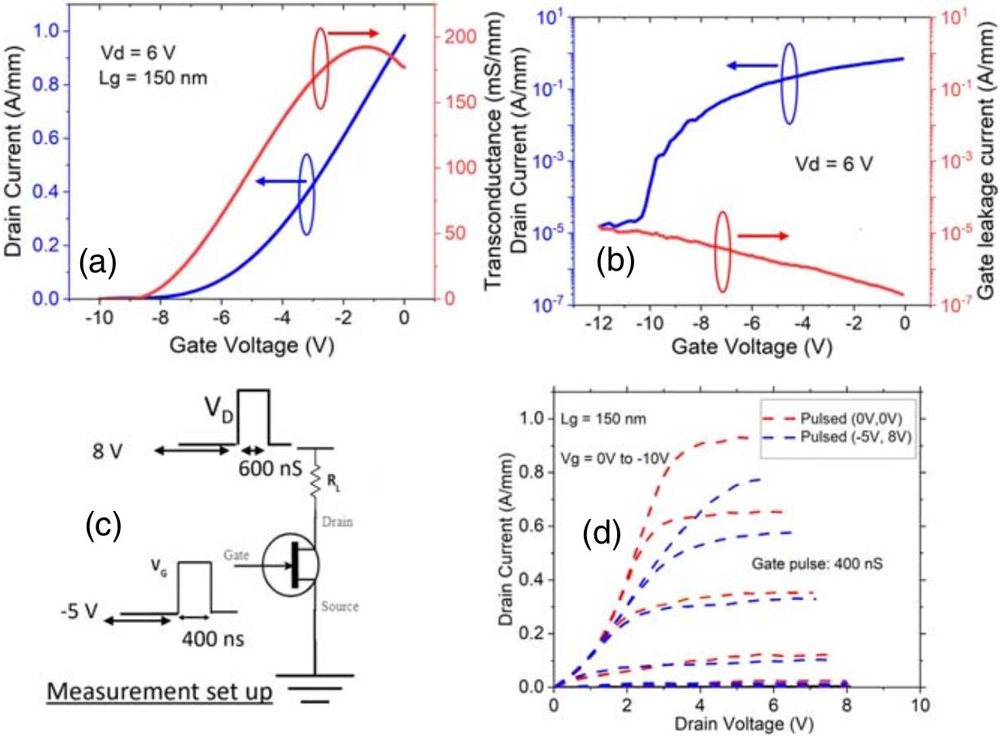
Figure 2: Transfer characteristics of the fabricated device with diamond deposited at 500°C in (a) linear scale and (b) semi-logarithmic scale. Measurement set-up (c) for comparison of output characteristics at DC and pulsed condition (d).
For the lower 500°C diamond layer the transistor had a −8V gate threshold (normally-on/depletion mode) and 190mS/mm peak transconductance (Figure 2). The on/off current ratio was 105, and the gate leakage was only 10μA/mm.
The researchers comment: “This shows the importance of low-temperature deposition technique for the successful demonstration of ‘device first’ all-around diamond integrated devices for device-level cooling solutions.”
The researchers used pulsed modes to assess the dispersion/current collapse performance of the MISHEMTs. The drain and gate pulse widths were 400ns and 600ns, respectively. The pulse period was 5ms. The drain saturation current was 0.96A/mm. The dispersion at the knee current level was around 20%.
The team comments: “The dispersion in this device is due to the lack of a deep recess structure with GaN cap layer and the absence of a field-plate structure.”
Diamond on GaN HEMT GaN HEMT AlGaN MOCVD
https://doi.org/10.35848/1882-0786/adcb87
The author Mike Cooke is a freelance technology journalist who has worked in the semiconductor and advanced technology sectors since 1997.


