


News: LEDs
30 October 2025
P-type layer etch for enhanced deep UV LEDs
Researchers in China have reported on the potential for enhancing the performance of aluminium gallium nitride (AlGaN) deep ultraviolet (DUV) light-emitting diodes (LEDs) by etching away DUV-absorbing portions of the hole injection structures [Hualiang Qiu et al, J. Appl. Phys., v138, p145702, 2025)].
DUV LEDs are being developed to replace mercury DUV sources for applications such as sterilization, medical treatment, and biological detection. The hope is to develop more efficient, compact, robust and environmentally friendly DUV sources.
Presently, DUV LEDs suffer from low wall-plug efficiency (WPE) due at least in part from low light-extraction efficiency (LEE). One of the main culprits for absorbing DUV is the p-type layers needed for hole injection into the light-emitting regions for recombination with electrons to produce DUV light.
The ohmic contact with metal electrodes needs p-GaN rather than p-AlGaN for hole injection. Unfortunately, p-GaN is highly absorbing of DUV, due to its bandgap energy (of order 3.4eV) being less than the DUV photon energy (280–200nm, 4.4–6.2eV).
Etching away the DUV-absorbing material can increase LEE, but at the cost of reducing the internal quantum efficiency (IQE) as a result of etching defects, and increased series resistance.
The team from Shanxi University, Hebei University of Technology, Institute of Semiconductors, University of Chinese Academy of Sciences, Advanced Ultraviolet Optoelectronics Co Ltd, and North University of China, comment: “The optimal p-type etching process for DUV-LEDs with an ultra-thin p-type layer must balance the enhanced LEE against the reduced IQE and carrier injection efficiency.”
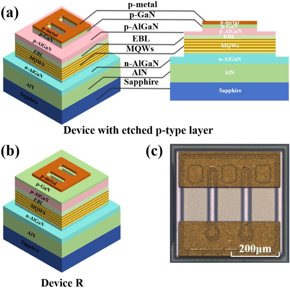
Figure 1: (a) Three-dimensional and cross-sectional schematics of DUV-LEDs with etched p-type layer (devices 1–3). (b) Three-dimensional schematic of conventional DUV-LEDs, reference ‘device R’. (c) Microscope image of conventional DUV-LED.
The AlGaN material for the DUV-LEDs (Figure 1) was grown using metal-organic chemical vapor deposition on sapphire. The active region was a five-period multiple quantum well (MQW) consisting of 3nm Al0.45Ga0.55N wells separated by 12nm Al0.56Ga0.44N barriers.
The magnesium-doped p-type layers were 40nm p-Al0.8Ga0.2N for the electron-blocking layer (EBL), 20nm AlGaN graded from 0.75% to 0.35% Al, and 2nm p-GaN. The researchers comment: “The entire p-type layer has a thickness of approximately 62nm, which is significantly thinner than typical values reported in studies on etched p-type layers.”
The DUV-LED began with patterning and inductively coupled plasma (ICP) etching of the device mesas. ICP etching was also used to remove part of the p-type layers in the non-contact region, aiming to increase the light output. The etch depth was varied by the etch durations: 2s, 3s and 6s for devices 1–3, respectively. Surface defects from the etching were removed using potassium hydroxide (KOH) solution.
The n- and p-metal electrodes were titanium/aluminium/nickel/gold and nickel/rhodium/nickel/gold, respectively. The p-ohmic contact was then annealed at 600°C for 13 minutes. A final metal sequence of aluminium/titanium/gold was formed into a reflector and to enhance current spreading.
The final steps were sapphire thinning to 400μm, and device separation into 20milx20mil (0.5mmx0.5mm) chips by laser stealth dicing. A conventional device without p-layer etching was also fabricated for reference (R) purposes.
Table 1: Optical, structural, and electrical performances.
Characteristic |
R | 1 | 2 | 3 |
| Transmittance (274nm wavelength) | 77.81% | 85.53% | 89.31% | 90.92% |
| Etch depth | 0nm | 7.5nm | 12nm | 18nm |
| Surface roughness of etched region | 9.36nm | 10.7nm | 11.0nm | 12.7nm |
| Voltage at 100mA current | 5.55V | 5.71V | 5.92V | 5.58V. |
| Series resistance | 6.83Ω | 9.06Ω | 11.92Ω | 8.14Ω |
| Premature turn-on | — | 4.1V | 3.7V | 3.3V |
| LOP at 100mA | 18.71mW | 19.49mW | 20.75W | 10.82mW |
| WPE at 100mA | 3.77% | 3.87% | 2.10% | 3.58% |
Various measurements were made such as transmittance to DUV, and atomic force microscopy (AFM) p-layer etch depth and root-mean-square (RMS) etch surface roughness (Table 1).
Electrical characterization was derived from current–voltage measurement (Figure 2). The degraded electrical performance of the p-etched devices was attributed to the reduced conductive volume from the p-etching. The premature turn-on was blamed on a parasitic diode with lower barrier height relative to the desired LED behavior under the p-etched region.
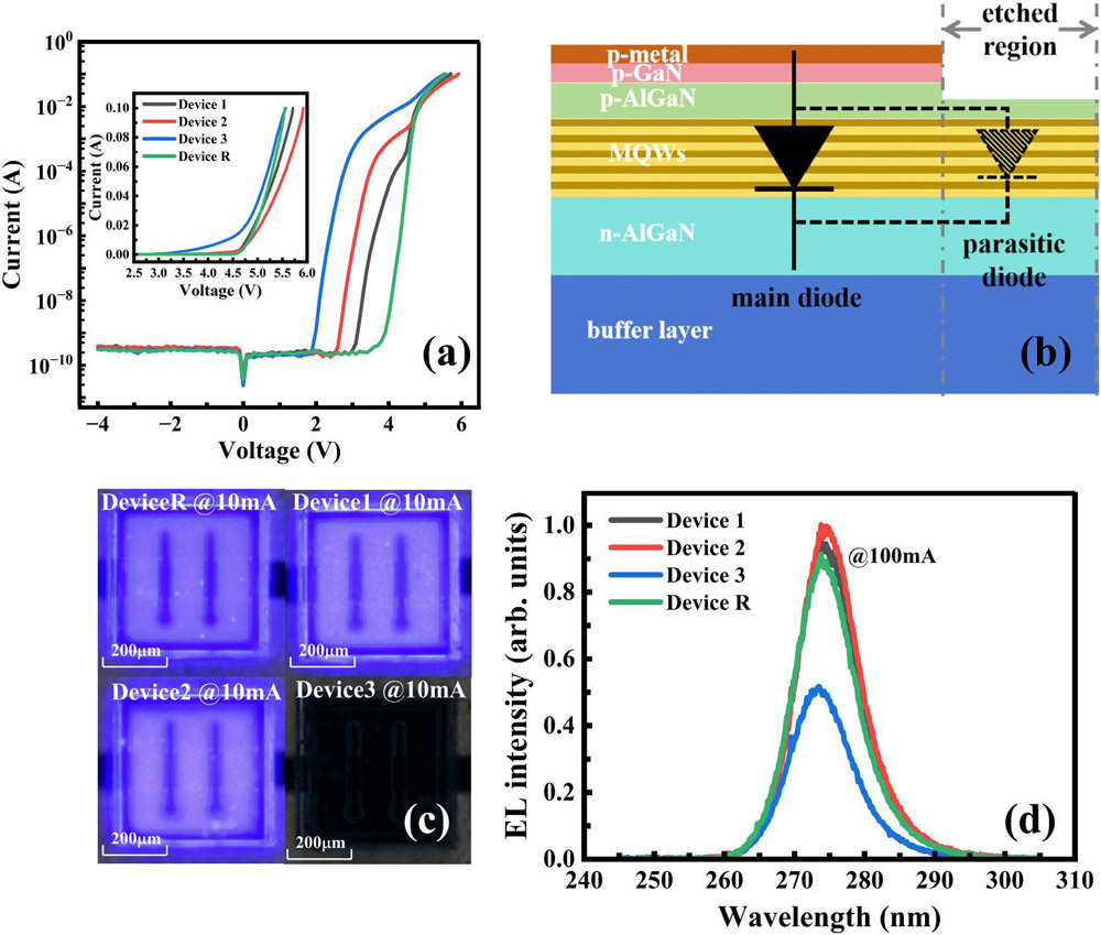
Figure 2: (a) Current–voltage curves of each device. (b) Schematic diagram of equivalent diode for p-GaN etched devices. (c) Luminescence photographs of devices at 10mA injection. (d) Electroluminescence (EL) spectra of device at 100mA injection.
The 18nm p-etching in device 3 did not even light up at 10mA injection due to the current leakage through the parasite. At 100mA, the light from device 3 was about half that of the others. The researchers also believe that the etch defects affect the internal quantum efficiency of the MQW active light-emission region, increasing the non-radiative Shockley–Read–Hall recombination mechanism rate, hence reducing IQE.
The team comments: “For the DUV-LEDs with an ultra-thin p-type layer, it is crucial to carefully control the etching of p-type layer to prevent the introduction of etching-induced defects into the active region.”
The light output power of device 2 showed the best performance while, for lower currents, device 1 had better wall-plug efficiency (Figure 3).
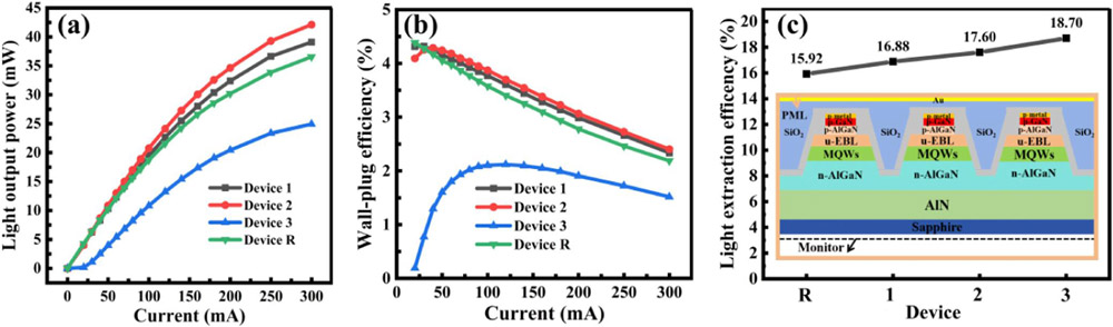
Figure 3: (a) Light output power (LOP) and (b) wall-plug efficiency (WPE) versus current. (c) Light extraction efficiency (LEE) versus etching depth, based on two-dimensional finite-difference time-domain (2D-FDTD) simulations.
The researchers comment: “It is evident that etching-induced defects propagate from the p-type layer surface into the active region with increased etching depth. These defects within the p-type layer adversely affect hole injection efficiency. Therefore, the degradation in WPE for device 3 can be attributed to the combined reduction of both IQE and hole injection efficiency. In addition, the highest WPE of device 2 is due to a high LEE and few etching defects in the active region.”
https://doi.org/10.1063/5.0291142
The author Mike Cooke is a freelance technology journalist who has worked in the semiconductor and advanced technology sectors since 1997.


