


News: Microelectronics
17 April 2026
Silicon aluminium nitride on GaN MISHEMTs for 6G and X-band
Japan’s Fujitsu Ltd has claimed the first silicon aluminium nitride (SiAlN) metal-insulator-semiconductor high-electron-mobility transistor (MIS HEMT) to achieve the coexistence of more than 70% power-added efficiency (PAE) and 10W/mm output power (Pout) in the 8–12GHz X-band [Yuichi Minoura et al, Applied Physics Express, v19, p021010, 2026].
The SiAlN combination is expected to have a high dielectric constant, intermediate between the values for AlN and SiN, with AlN tending to be higher than SiN’s value of about 8. A high-dielectric-constant gate stack should suppress effects that degrade transconductance performance.
High-efficiency and high-power X-band HEMTs have potential for microwave power amplifiers. The 8GHz performance of the Fujitsu HEMTs also falls in the third frequency range (FR3, 7.125–24.25GHz) proposed for 6G mobile communications. This would add to the 5G FR1 (0.410–7.125GHz) and FR2 (24.25–71.0GHz) ‘New Radio’ (NR) bands.
Other uses for X-band devices with high efficiency and power ratings would include defense and meteorological applications for radar systems with varying long detection range and high resolution combinations in compact form factors.
The researchers comment: “For these applications, it is crucial to achieve both high output power and efficiency in power amplifiers to ensure communication range, reduce power consumption, and simplify cooling mechanisms.”
The MIS structure is needed to reduce the performance impacts of gate leakage and constrained gate voltage swing. The team reports: “Until now, satisfactory MIS HEMTs operating at ultra-high speeds in the GHz range have not been realized due to issues with the quality of the gate dielectric film itself and the GaN-based semiconductor interface.”
The researchers comment that increasing output power by increasing the gate width runs into problems at high frequency: “We believe that increasing the total gate width by increasing the gate width per finger or the number of gate fingers leads to problems such as an increase in gate resistance and phase misalignment within the same device when the device size becomes larger. Therefore, we prefer to increase the output power density, assuming sufficient heat dissipation, and have pursued research and development with a target of 10W/mm.”
The epitaxial material for the device was grown by metal-organic chemical vapor deposition (MOCVD) on a hydride vapor phase epitaxy (HVPE) semi-insulating GaN substrate (Figure 1).
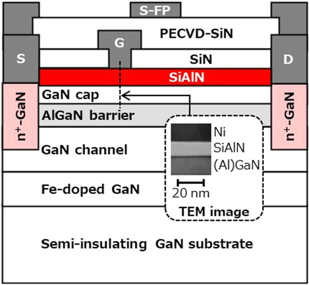
Figure 1: Cross-sectional GaN SiAlN MIS HEMT scheme. Inset: transmission electron microscope (TEM) image of gate cross-section.
The 10nm SiAlN gate insulator was also grown by MOCVD, immediately after the semiconductor layers. The SiAlN also provided passivation. The Si:Al ratio was found to be 77:23, according to x-ray photoelectron spectroscopy (XPS) analysis.
The researchers comment: “Depositing the SiAlN just after epitaxial growth can reduce damage to the GaN-based semiconductor from subsequent device processing, such as plasma or wet chemical treatments.”
The SiAlN was then covered with SiN with a view to preventing degradation of the upper interface of the SiAlN during subsequent device processes and as part of a gate field-plate (FP). The SiAlN also served as an etch stop for the gate recess dry etch with a selectivity ratio of 2.8 for SiN over the SiAlN.
A post-deposition sheet resistance study on epitaxial structures with the SiAlN dielectric gave a value of 339Ω/□, compared with 348Ω/□ for SiN only.
The ohmic source/drain electrodes were recessed with re-grown heavily doped n-GaN also applied using MOCVD. The ohmic metal contacts were titanium/aluminium. The gate metal was nickel/gold. The gate length was 0.2μm. A source FP was also constructed using a plasma-enhanced chemical vapor deposition (PECVD) SiN spacer.
Compared with a Schottky gate structure, the SiAlN MIS HEMT showed up to four orders of magnitude lower reverse and forward gate leakage current in two-terminal gate measurements. The turn-on gate voltage was increased from 0.8V for the Schottky structure to 4V for the MIS HEMT. The higher turn-on should enable a higher input voltage swing. The reverse breakdown occurred at 384V, compared with 194V for a Schottky HEMT.
Three-terminal measurements gave a maximum transconductance (gmmax) of 258mS/mm at 10V drain bias, compared with 338mS/mm for the Schottky HEMT.
The researchers comment: “Although the SiAlN MIS HEMT exhibited a lower gm due to the presence of the gate dielectric, its deeper Vth enabled a larger Id of 1325mA/mm at a gate voltage (Vgs) of +2V, compared to 1069mA/mm for the Schottky HEMT.”
The threshold voltages (Vth) for the MIS and Schottky HEMTs were −5.81V and −2.42V, respectively. At +4V gate potential the drain current of the MIS HEMT reached 1404mA/mm, promising for increased output power density.
The threshold shift during −0.5V/s downward gate sweeps was 25mV. “This remarkably small dependence of Vth on the positive gate bias pre-stress indicates the high quality of both the gate dielectric and the dielectric/semiconductor interface,” the team reports.
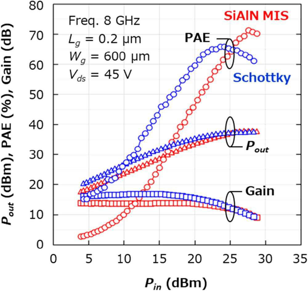
Figure 2: Power characteristics of Schottky and SiAlN MIS HEMTs by on-wafer load-pull measurements in pulse mode at 8GHz.
The researchers performed load-pull measurements with 1% duty cycle for pulsed operation (Figure 2). At 8GHz, the power-added efficiency reached 74.3%, when the impedance matching was optimized for efficiency. The corresponding output power (Pout) was 9.8W/mm. With impedance matching aimed at high output power (Pout) the SiAlN HEMT achieved 10.4W/mm, along with 71.4% PAE. The reference Schottky HEMT only managed 66.0% PAE and 8.9W/mm Pout.
To explore performance in the S-band, also used in wireless communications and radar, the researchers reduced the frequency to 3GHz. The PAE increased to 80.6% with Pout also increasing slightly to 10.5W/mm. Thus, the researchers conclude that the SiAlN MIS HEMT structure could offer performance operation across a wide range of frequencies.
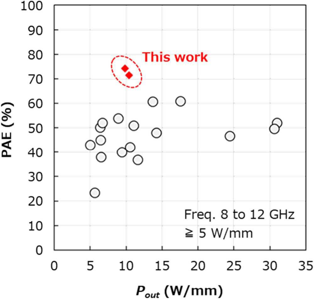
Figure 3: Benchmark of maximum PAE and output power density for GaN-based HEMTs exhibiting 5W/mm at X-band.
The researchers present a benchmark plot to compare with previous reports (Figure 3).
Silicon aluminium nitride GaN MISHEMTs GaN MIS HEMT PECVD MOCVD
https://doi.org/10.35848/1882-0786/ae428a
The author Mike Cooke is a freelance technology journalist who has worked in the semiconductor and advanced technology sectors since 1997.


