

News: Microelectronics
27 August 2026
Thin p-GaN ohmic contact formation
Researchers based in Japan, USA and China propose an improved process for thin p-type gallium nitride (GaN) ohmic contacts by ultrathin magnesium (Mg) deposition and brief thermal annealing [Haitao Wang et al, Appl. Phys. Lett., v129, p063306, 2026].
The team from Nagoya University, Cornell University, University of Illinois Urbana-Champaign, Massachusetts Institute of Technology, City University of Hong Kong, and Suzhou Institute of Nano-Tech and Nano-Bionics, reports:
“We demonstrate that a bare sub-10nm Mg layer followed by a brief and mild anneal (600°C and 300s) forms an ultra-shallow acceptor-rich region in thin p-GaN while preserving the surface morphology. The resulting contacts exhibit a zero-bias specific contact resistivity in the low-10−4Ω-cm2 range, retain p-type Hall transport and favorable mobility, and enable improved forward carrier injection without compromising reverse blocking.”
Forming ohmic contacts on p-GaN is tricky due to the deep ~200eV Mg acceptor ionization energy, along with the tendency of subsequent plasma etch to introduce defects with compensating donor energy states. To overcome this bottleneck, the surface p-GaN is typically heavily doped through epitaxial regrowth or ion implantation, adding to process complexity, and production costs. Such processes also come with the risk of structural damage that may need further annealing processing, increasing the thermal budget.
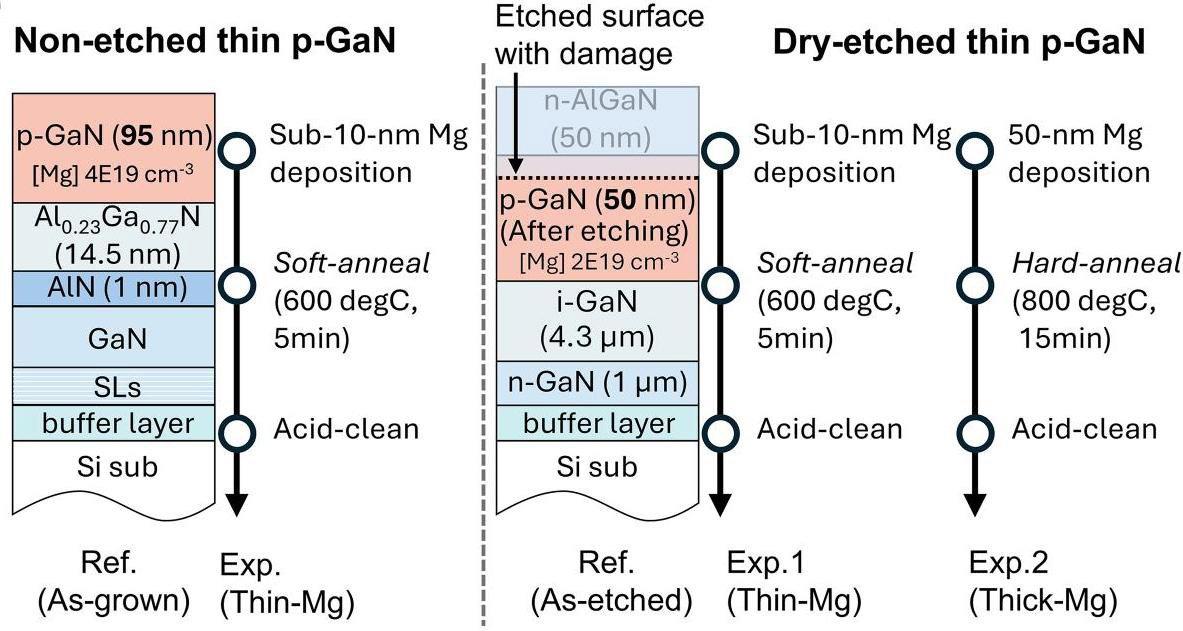
Figure 1: Process routes for non-etched thin p-GaN/AlGaN heterostructure and dry-etched thin p-GaN homojunction samples.
The researchers tested their technique on two samples reflecting typical device scenarios (Figure 1): p-GaN gate high-electron-mobility transistors (HEMTs) and GaN npn heterostructure bipolar transistors (HBTs). For the p-GaN gate, the magnesium was directly deposited on the surface p-GaN, while for the HBT the top n-type aluminium gallium nitride (AlGaN) layers have to be etched away to provide access to the p-GaN base contact.
A typical problem with etching, particularly with ‘dry’ plasma etching, is that it leaves a rough surface that can create downstream processing and device performance challenges. The team used chlorine-based reactive-ion etch (RIE) to remove the n-AlGaN and 20nm of the 70nm p-GaN layer.
Magnesium was deposited on these surfaces via magnetron sputtering. A 90 second sputter process at 50W power deposited around 8–9nm of Mg. Increasing to 900s sputtering, the Mg layer grew to ~50nm. These layers were exposed to the atmosphere for several hours before annealing. No capping layer was used to protect the Mg during this period. The 900s thicker Mg layer is typical of previous work aimed at giving heavy surface doping in thicker p-GaN layers.
The post-anneal cleaning consisted of a dilute solution of hydrochloric acid and hydrogen peroxide to remove surface Mg residues and amorphous oxide.
X-ray photoelectron spectroscopy (XPS) analysis showed that one result of ‘soft’ annealing was to reduce the surface valence band bending to 1.3eV, compared with 2.2eV for ‘hard’ annealing, consistent with simulations. The researchers say that this indicates a reduced effective hole-injection barrier and a narrowed depletion region near the metal interface.
The team found no evidence of Mg segregation, Mg intercalation, or Mg-intercalated GaN superlattice (MiGs) formation (MgGaN) in transmission electron microscope (TEM) analysis.
The researchers comment: “This behavior differs from our previous studies employing thick-Mg layers and higher thermal-budget annealing conditions (hard annealing), in which Mg intercalation and MiG formation were frequently observed. Those structures were accompanied by pronounced Mg accumulation, with Mg concentrations approaching ~1022/cm3 in the back-side secondary-ion mass spectrometry (SIMS) profiles.”
The researchers performed 10μm×10μm and 2μm×2μm AFM scans at various steps (Figure 2). The root-mean-square roughness over the 10μm field was 0.25nm as-grown, 1,59nm as-etched, 1.56nm thin-Mg soft annealing, and 18.22nm thick-Mg hard annealing. For the smaller field the corresponding values were 0.17nm, 1.51nm, 1.47nm and 20.90nm. Unlike the other samples, the thick-Mg hard annealing showed an increased roughness for the 2μm due to the increased resolution of agglomerated, cauliflower-like features.
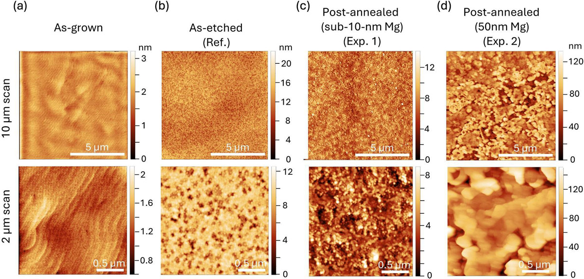
Figure 2: Atomic force microscope (AFM) topography of (a) as-grown, (b) as-etched, and post-annealed (c) sub-10nm Mg and (d) 50nm Mg on p-GaN.
The researchers comment: “Such pronounced roughness can broaden the effective interface thickness, promote local current crowding under the contact, and introduce non-uniformity during subsequent metal deposition. We also investigated the effect of low-temperature annealing on the surface morphology. Even after annealing at 500°C, the surface remained rough. This suggests that the degradation of the thick-Mg samples cannot be attributed solely to the high annealing temperature. Rather, the large Mg thickness itself plays a critical role in causing severe surface degradation and poor contact performance.”
Electrical performance was assessed using circular transfer length method (CTLM) patterns in annealed nickel/gold metal stacks. By varying the pattern dimensions, sheet (Rsh) and contact (Rc) resistances could be extracted.
The thin Mg samples showed much reduced specific contact resistivity (ρc) in both voltage and current sweeps. For the dry-etched surfaces the ρc was less than 2.04×10⁻⁴Ω-cm2 (at 0V), while for non-etched p-GaN the peak ρc value was slightly higher at 2.74×10⁻⁴Ω-cm2 (0.1mA). For what it is worth, the lowest non-etched value was 1.26×10⁻⁴Ω-cm2 (2V), while the etched p-GaN reached as low as 3.54×10⁻⁵Ω-cm2 (0.2mA).
The researchers comment: “For the thin-Mg soft-annealed samples, the extracted ρc values from voltage- and current-sweep measurements remain close to each other, indicating a nearly intrinsic Ohmic contact state with good reproducibility. This suggests that current conduction is mainly governed by direct tunneling under reverse-biased conditions at the metal/p-GaN contact. By contrast, the discrepancy becomes much larger for the as-etched and thick-Mg hard-annealed samples, where nonlinearity, local non-uniformity, and stronger bias dependence are observed.”
The ρc for the other cases, i.e. as-grown and thick Mg, was at least an order of magnitude higher, even up to eight orders for as-etched material.
The impact of the different processes was also revealed by Hall measurements. Thin Mg annealing resulted in a sheet resistance (Figure 3) of 3.30×10⁵Ω/□, compared with 1.09×10⁷Ω/□ for the thick-Mg process. The researchers see the degradation in the latter case stemming from serious non-uniform thinning of the p-GaN by the thick-Mg annealing process, “consistent with severe surface roughening and spatial variations in the post-annealed p-GaN layer.”
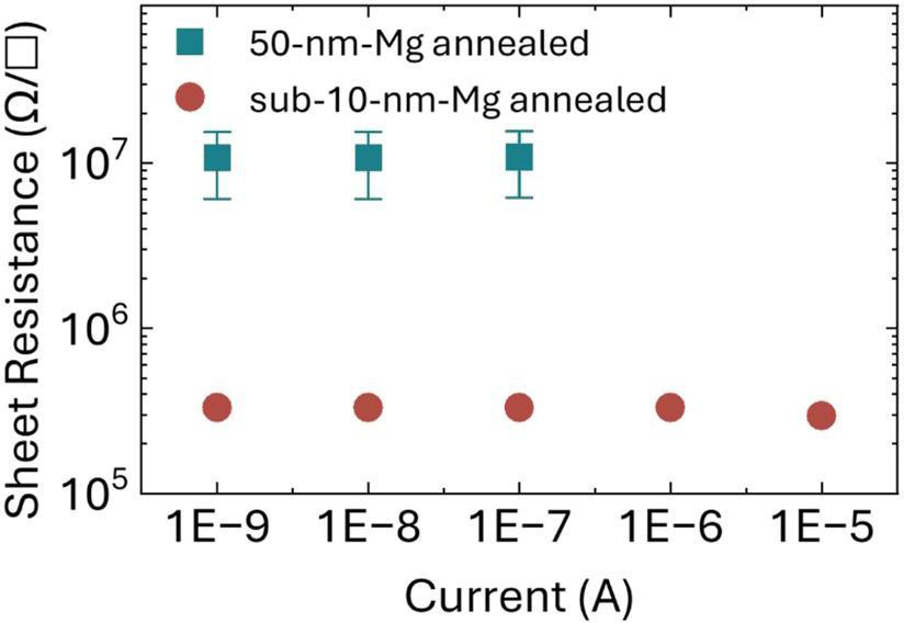
Figure 3: Hall sheet resistance measured by van der Pauw method for thick Mg and thin Mg samples.
The researchers also fabricated quasi-vertical p–i–n diodes based on different samples (Figure 4). The reference devices were fabricated using as-etched samples. Mesa isolation was through RIE. The anode and cathode were sintered nickel/gold (Ni/Au) and as-deposited chromium/gold (Cr/Au), respectively. The etched mesa sidewalls were passivated with polyimide.
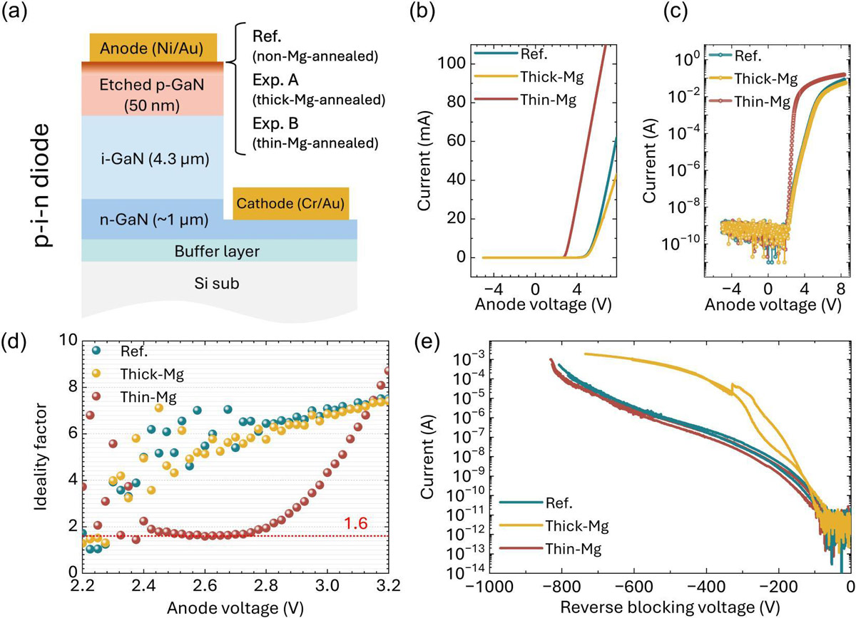
Figure 4: (a) Quasi-vertical p–i–n diodes. Forward current–voltage characteristics on (b) linear and (c) semi-log scales, along with (d) the extracted ideality factor. (e) Reverse characteristics.
The process order had to be varied between the thin and thick Mg annealing processes. The annealed thin Mg anode formation could be performed before the mesa isolation. The thick Mg required a reversal in these steps.
The team explains: “This difference arises because the severe surface roughening induced by thick-Mg annealing hinders subsequent mesa etching, whereas the smooth surface after thin-Mg annealing enables clean mesa formation with well-defined sidewalls. This also highlights a practical advantage of the thin-Mg process, as blanket Mg deposition eliminates the photolithography and lift-off steps for Mg patterning, thereby reducing process complexity and potential photoresist contamination.”
The turn-on voltage of the thin Mg diode was 3V, significantly lower than the reference and thick Mg devices. Further, the thin-Mg diode demonstrated a 0.32V range of near-ideal (1.6) characteristics, “indicating stable near-diffusion-limited transport with suppressed Shockley–Read–Hall recombination, consistent with a high-quality junction and contact”.
The reverse current leakage of the thin Mg and reference devices were much lower than for the thick-Mg diode. The breakdown voltage of the thin-Mg device therefore exceeded 800V.
GaN ohmic contacts GaN Magnesium deposition HEMTs HBTs
https://doi.org/10.1063/5.0339815
The author Mike Cooke is a freelance technology journalist who has worked in the semiconductor and advanced technology sectors since 1997.