

News: Microelectronics
6 August 2026
Taking heat off AlGaN-channel HEMTs
Pennsylvania State University (PSU) and Cornell University in the USA claim record-high thermal performance for an ultra-wide-bandgap aluminium gallium nitride (AlGaN)-channel high-electron-mobility transistor (HEMT) [Seokjun Kim et al, IEEE Electron Device Letters, published online 20 April 2026]. The team reports around 20% lower channel temperature rises compared with a conventional GaN HEMT on silicon carbide (SiC) substrate.
Although AlGaN channels should provide attractive properties for power and wireless electronics, such as supporting higher breakdown fields, the low thermal conductivity of the material raises concerns for device overheating and thermal failure.
Alloyed materials like AlGaN (alloy of AlN and GaN) with an irregular crystal structure tend to have lower thermal conductivity due to increased phonon scattering impeding heat flow.
For example, Al0.25Ga0.75N films have a thermal conductivity around 10W/m-K, compared with 155W/m-K for GaN. For Al contents up to 85%, the conductivity remains in the range 8.5–10.0W/m-K.
The problem is even worse if sapphire with around 35W/m-K thermal conductivity is used as the substrate. PSU/Cornell have performed simulations that suggest that using SiC, with around 350W/m-K conductivity, instead of sapphire as substrate reduces the total AlGaN HEMT thermal resistance by 89%.
The PSU/Cornell device reduced the thickness of the AlGaN layer used as the channel to 24nm by growing it pseudomorphically on AlN rather than having an AlGaN buffer layer. An added advantage of the AlN buffer is that it acts as a back-barrier, suppressing vertical leakage currents and preventing vertical breakdown.
Based on their work, the team suggests three thermal design rules:
“(i) The AlGaN-channel/buffer should be grown on (or integrated with) a high-κ substrate serving as a heat sink.
“(ii) The thickness of the low-κ AlGaN layer should be minimized via pseudomorphic growth.
“(iii) The buffer layer underneath the AlGaN channel should be replaced by a high-κ insulator, which serves as a near-junction heat spreader.”
One should perhaps point out that “κ” (Greek kappa) here refers to thermal conductivity, NOT dielectric constant.
The team also sees the ultra-thin pseudomorphic channel as providing improved electron confinement and gate modulation, mitigating short-channel effects. This would bring advantages for ultra-scaled AlN/AlGaN/AlN-on-SiC HEMTs in terms of improved radio frequency (RF) output power, efficiency, and device reliability, enabled by the lower junction temperature, higher critical electric field, and comparable electron saturation velocity to GaN-channel devices.
The researchers comment: “The thermal performance of AlN/AlGaN/AlN HEMTs can be further improved by adopting either an AlN substrate by taking advantage of bulk-like heat conduction through the AlN buffer/substrate or a diamond substrate by exploiting its highest κ.”
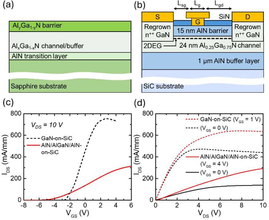
Figure 1: Cross-sectional schematic of (a) conventional epitaxial material stack for AlGaN-channel HEMT and (b) PSU/Cornell’s AlN/AlGaN/AlN-on-SiC HEMT. Comparison with GaN-on-SiC HEMT: (c) electrical transfer and (d) output characteristics.
The material for the HEMT was grown on commercial 6H-SiC substrate by molecular beam epitaxy (Figure 1). Hall measurements of the two-dimensional electron gas (2DEG) characteristics showed a carrier density of 3.05×10¹³/cm2 at 300K.
The source and drain contacts consisted of heavily doped n++-GaN to reduce the electrical channel access resistance. The gate length (Lg) was 1.5μm. The distances of the gate from the source (Lsg) and drain (Lgd) were 1.25μm and 2.25μm, respectively. The channel width was 50μm. Silicon nitride (SiN) provided passivation.
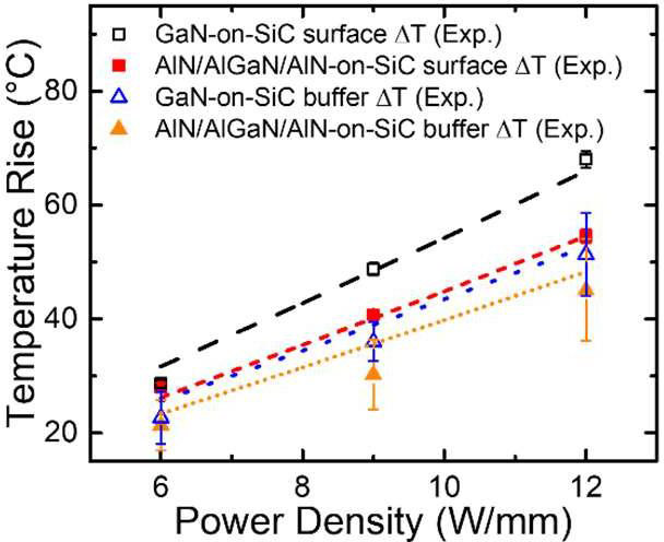
Figure 2: Measured (points with error bars denoted as “Exp.”) and simulated (lines) surface (or channel) and buffer temperature rises (ΔT) of AlN/AlGaN/AlN-on-SiC and conventional GaN-on-SiC HEMTs.
The temperature rises were extracted using Raman spectroscopy techniques (Figure 2). The AlGaN-channel device showed around 12% and 20% lower respective buffer and surface temperatures than the conventional GaN-channel HEMT at 12W/mm power density.
https://doi.org/10.1109/LED.2026.3684862
The author Mike Cooke is a freelance technology journalist who has worked in the semiconductor and advanced technology sectors since 1997.