

News: Optoelectronics
5 August 2026
Blue photonic crystal surface-emitting laser
Researchers based in China report a room-temperature blue gallium nitride (GaN)-based photonic crystal surface-emitting laser (PCSEL) diode realized by regrowth-free fabrication [Zhiwei Sun et al, Appl. Phys. Lett., v128, p243310 2026].
“A critical advantage of PCSELs is their ability to produce high-quality beams with low divergence,” comments the team from Suzhou Laboratory, University of Science and Technology Beijing, Suzhou Institute of Nano-Tech and Nano-Bionics, Xi’an Jiaotong-Liverpool University, and Suzhou Ganbright Optoelectronic Technology Co Ltd.
The researchers report an extremely low divergence angle for their device of 0.066°. Edge-emitting lasers suffer from wide divergence with an elliptical rather than circular profile. Vertical-cavity surface-emitting lasers (VCSELs) have been commercialized at infrared wavelengths, but implementation of the concept for visible blue laser light is challenging due to material limitations.
Photonic crystal (PhC) structures offer opportunities to overcome some of these limitations. The researchers comment: “The multi-directional distributed feedback effect near the band edge allows for the formation of a coherent large-area standing wave, while first-order diffraction from the grating enables surface emission. This mechanism allows PCSELs to achieve high-power, single-mode lasing with a very narrow divergence angle and high brightness, as has been extensively demonstrated in III–V arsenide and phosphide materials.”
There have been some reports of the GaN-based PCSELs, but these typically use epitaxial regrowth steps during fabrication, which increases process complexity and cost. Another complicating factor is the use of double-lattice structures to enhance beam quality for very large devices, requiring difficult lithography and etching sequences. The researchers here instead used a single lattice, hoping that this would be sufficient for compact devices.
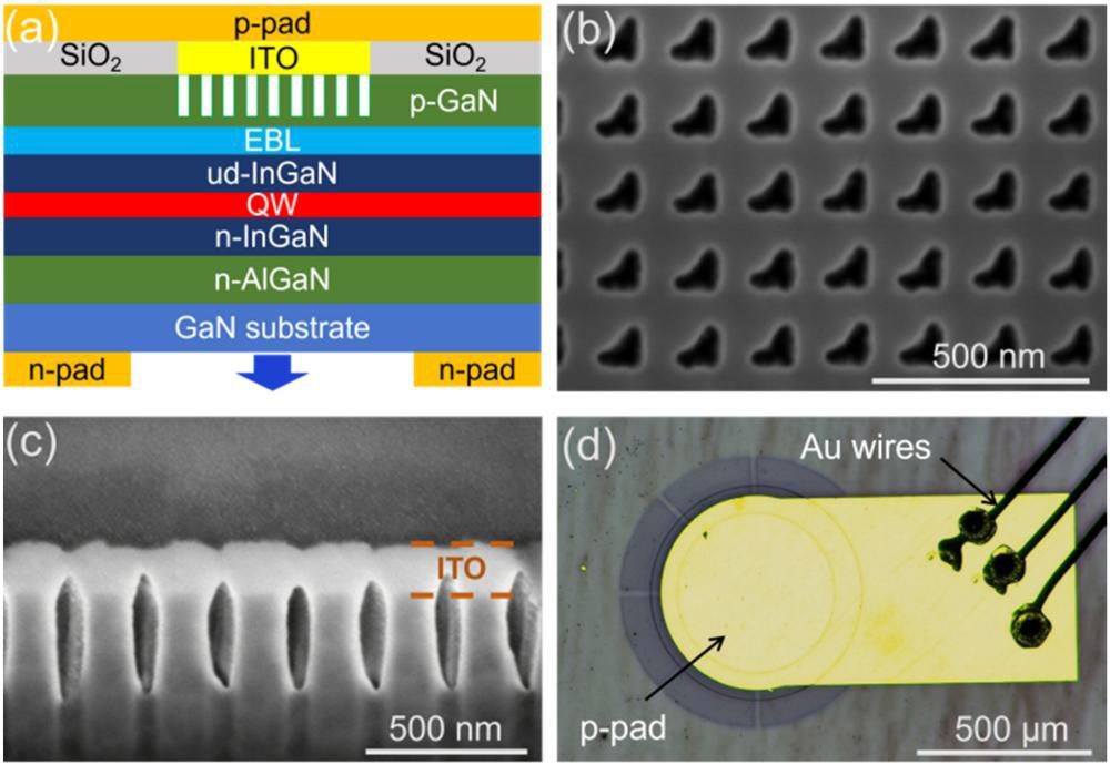
Figure 1: (a) Schematic diagram of GaN PCSEL. White bars represent air holes of PhC. (b) Scanning electron microscope (SEM) image of square lattice with air holes. (c) Cross-sectional SEM image after ITO deposition. (d) Top-view microscopy image of finished device.
The epitaxial material for the device (Figure 1) was grown by metal-organic chemical vapor deposition (MOCVD) on GaN substrate. The laser light was designed to be emitted from the bottom surface. The layer sequence was: 1.9μm n-type aluminium gallium nitride (n-AlGaN) cladding, 100nm indium gallium nitride (n-InGaN) waveguide, 5nm/12nm In0.12Ga0.88N single quantum well (QW), 100nm undoped InGaN waveguide, 20nm AlGaN electron-blocking layer (EBL), and 475nm p-GaN cladding.
The researchers comment on the p-GaN: “This layer replaces the AlGaN cladding conventional to edge-emitting laser diodes to facilitate photonic crystal etching and electrical contact formation.”
The fabrication avoided regrowth steps to facilitate process simplicity. The PhC consisted of a square lattice with isosceles right triangle air holes etched in the p-GaN by inductively coupled plasma. The lattice constant was 174nm to match the modal index of the fundamental guided mode. The circular PhC area was of 600μm diameter. The air holes present a high refractive index contrast with GaN.
The p-side electrode consisted of transparent indium tin oxide (ITO) with a diameter only slightly exceeding the PhC area to reduce current waste through the structure. Plasma-enhanced chemical vapor deposition (PECVD) silicon dioxide (SiO2) electrically isolated the device.
The PCSEL was completed with a p-metal contact pad, thinning of the substrate, and n-metal deposition.
The researchers used pulsed operation to avoid self-heating effects. The team reports: “A distinct lasing peak emerges near 434nm at an injection current of 13.8A, with full lasing established at 14.8A. The spectral linewidth (FWHM) of the lasing peak is measured to be 25pm, a value limited by the resolution of our spectrometer.” The threshold current density was 5.2kA/cm2.
The slope efficiency of 6W/A is described as “limited”. The blame is apportioned to suboptimal coupling of the PhC to the vertical radiation mode, resulting in lateral dissipation of photons generated in the QW.
The team suggest possible efficiency improvements: “According to three-dimensional coupled-wave theory, shifting the PhC layer closer to the peak of the optical field to increase the vertical confinement factor (ΓPhC) will simultaneously enhance vertical radiation and suppress lateral loss.”
Practical steps towards this could include reducing the p-cladding thickness to boost PhC-optical field interaction, and p-cladding doping profile optimization to mitigate intrinsic optical losses.
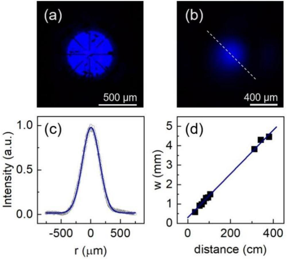
Figure 2: (a) Near-field pattern captured above threshold at 17.1A (6.05kA/cm2). Eight metal fingers extend from n-electrode toward center. Dark spot scattering is solder paste from PCB mounting. (b) Far-field pattern. (c) Intensity profile along dashed line in (b). Blue curve indicates Gaussian fit. (d) Position-dependent spot size (full width at 1/e2 intensity).
The far-field beam divergence was 1.15mradians (0.066°) with a Gaussian profile (Figure 2). The researchers attribute this exceptionally low value partially to single-mode operation at low power densities. The result is all the more remarkable given the relatively large 600μm diameter of the device.
The team writes: “This result highlights the ability of the photonic crystal cavity to maintain a coherent phase front over a large area, a capability that is difficult to achieve with conventional VCSELs or EELDs.”
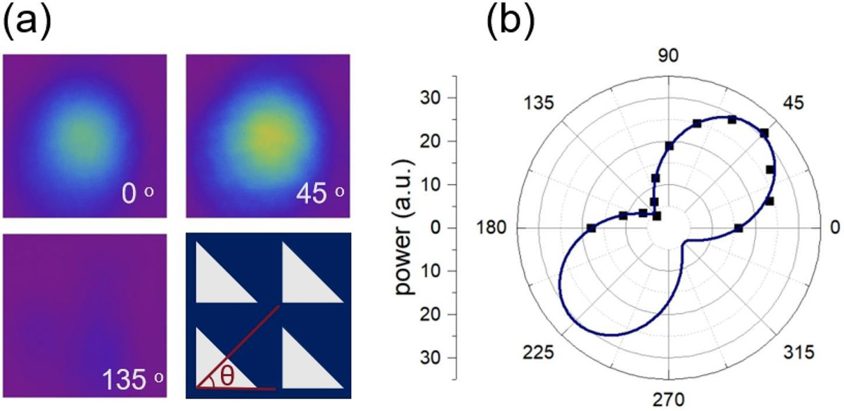
Figure 3: Far-field pattern and polarization characteristics at 21.4A (7.56kA/cm2): (a) contour plots with polarization filter at different angles θ. (b) Polar plot of light power versus polarization angle. Blue line represents best-fit sinusoidal curve.
The researchers also found the light output to be linearly polarized (Figure 3): “The polarization axis is oriented at 45°, which corresponds geometrically to the direction perpendicular to the long edge (hypotenuse) of the isosceles right triangular air holes. This polarization pinning is a direct result of the symmetry breaking introduced by the triangular air holes.”
https://doi.org/10.1063/5.0315502
The author Mike Cooke is a freelance technology journalist who has worked in the semiconductor and advanced technology sectors since 1997.