


News: Microelectronics
26 February 2026
GaN-on-silicon HEMTs for millimeter-wave 5G
Researchers based in Singapore and Belgium have reported record high peak power-added efficiency (PAE), of more than 60%, for moderately scaled gallium nitride (GaN) on silicon (Si) high-electron-mobility transistors (HEMTs) at 30GHz operation [Yihao Zhuang et al, IEEE Electron Device Letters, published online 22 January 2026]. At the same time, the devices perform with state-of-the-art noise figures (NFs) as low as 1.1dB.
The team from Nanyang Technological University, Agency for Science, Technology and Research (A*STAR), and Soitec Belgium/Singapore, comments: “These results suggest that moderate scaling could deliver competitive GaN-on-Si HEMT technology, when combined with optimized epitaxial structure and process.”
The researchers see the low-voltage (3–6V) RF devices as being suitable for monolithic integrated mobile transmit/receive (T/R) modules for the 5G high-frequency, mm-wave range (FR2, 24.25–71.0GHz). The low 5G range, FR1, covers 410–7125MHz. A proposed FR3, apparently not yet official, would bridge the gap between FR1 and FR2, i.e. 7.125–24.25GHz.
The team points out that existing technologies such as silicon germanium heterostructure bipolar transistors (SiGe HBTs) and gallium arsenide pseudomorphic HEMTs (GaAs pHEMTs) struggle to meet the stringent requirements for FR2. The high-volume mobile device market needs the low-cost and mass-production scale that could come from achieving high performance on GaN-on-Si HEMT platforms.
The researchers also comment on the benefit of moderate (around 100nm gate length) versus aggressive scaling: “Scaling down brings challenges in mass manufacturability on top of the limitations of the short-channel effect and reliability. Key characteristics for low-voltage operation, such as contact resistance, electron confinement, and trapping effects, can also be significantly improved through optimization of the epitaxial structure and fabrication process.”
The GaN material for the devices (Figure 1) was grown on high-resistivity silicon (Si) by metal-organic chemical vapor deposition (MOCVD). The structure included back- and top-barriers consisting of aluminium gallium nitride (AlGaN) and indium aluminium nitride (InAlN) alloys, respectively.

Figure 1: GaN-on-Si HEMT: (a) device structure; (b) transmission electron microscopy (TEM) image of T-gate and bilayer passivation.
The researchers comment: “The InAlN barrier provides strong polarization and a low gate-to-channel distance, enabling improved two-dimensional electron gas (2DEG) control. Additionally, the configuration of the ultra-thin GaN channel and the AlGaN BB further enhances electron confinement, effectively suppressing short-channel effects and lowering channel noise.”
The 80nm-deep n-GaN source/drain contact regions were grown by 725°C molecular beam epitaxy (MBE). The T-gate consisted of nickel/gold. The passivation was a bilayer of 250°C atomic layer deposition (ALD) aluminium oxide (Al2O3, 10nm) and 300°C plasma-enhanced CVD silicon nitride (60nm), aimed at suppressing surface trapping and leakage.
The researchers report that the passivation effectively reduced current collapse from more than 80% down to 24% in a 150nm gate-length (Lg) device. Gate lag was 10%. The HEMT’s other measured characteristics were 1.58A/mm maximum drain current, 1.48Ω-mm on-resistance, threshold voltage −2.9V, and 0.52S/mm peak transconductance at 6V drain bias.
For the small-signal frequency performance the researchers report for a 100nm-gate HEMT cut-off (fT)/maximum oscillation (fmax) respective values of 100GHz/254GHz at 10V drain. The fmax value for 5V drain was still more than 200GHz.
The researchers add: “The Lg = 150nm device still achieves an excellent fmaxxLg of 34.9GHz-μm which is comparable to the highest reported values obtained from extremely scaled GaN-on-Si HEMTs.”
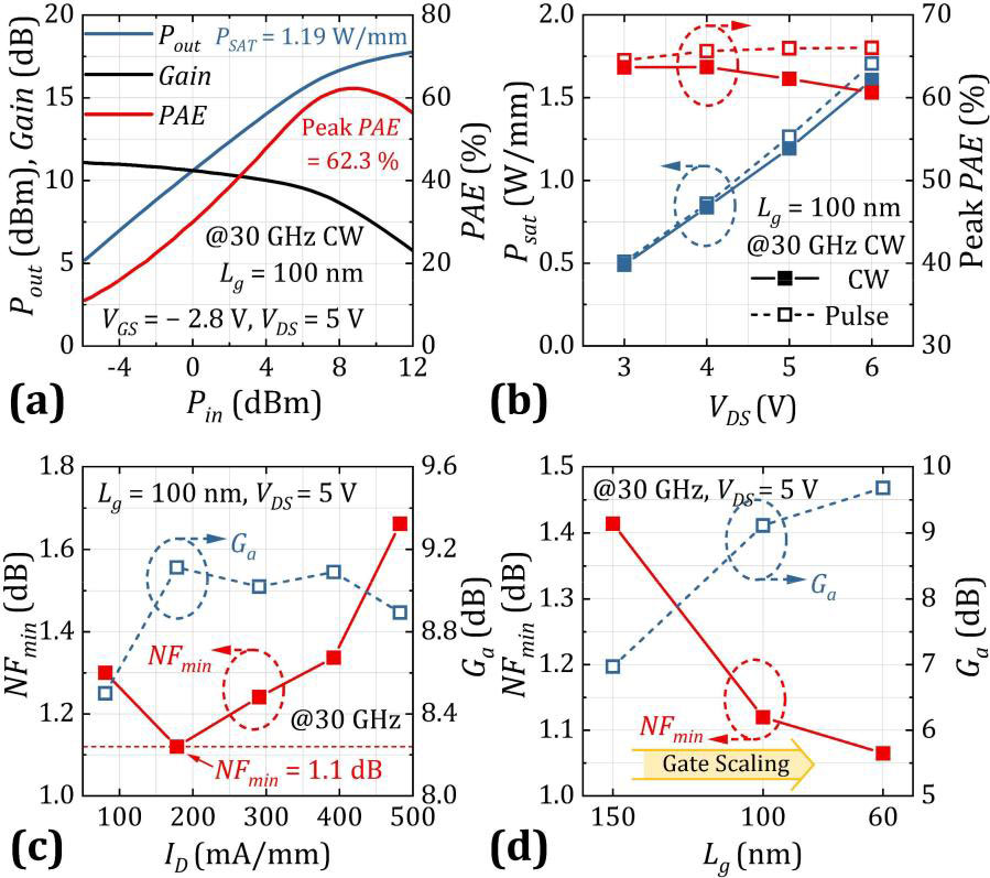
Figure 2: Power and noise performance of 100nm-gate device at 30GHz: (a) power performance at 5V drain; (b) saturated power (Psat) and peak power-added efficiency (PAE) versus drain bias (VDS) in both continuous wave (CW) and pulsed modes; (c) minimum noise figure (NFmin) and associated gain (Ga) versus drain current (ID), (d) improvement of noise performance from Lg scaling.
The PAE of a 100nm-gate device exceeded 60% across the 3–6V low-voltage range (Figure 2). The peak occurred at 63.7% at 3V and 4V.
“Thanks to the effectiveness of the proposed bilayer passivation in suppressing surface trapping effects, no significant difference in performance is observed between CW and pulsed modes,” the team comments.
The linear gain varied with Lg from 10.8dB at 150nm gate, through 11.1dB at 100nm, down to 14.7dB at 60nm. The researchers comment: “The high efficiency in low-voltage operation proves its potential for mobile applications.”
The researchers explain the low-noise performance measured in a cold-source system: “The excellent electron confinement, high gain, and low parasitic resistance, enabled by the ultra-thin channel, AlGaN BB, and regrown ohmic contacts, result in outstanding low-noise characteristics (NFmin < 1.4dB) across FR3 to FR2 bands from 10GHz to 40GHz, even without aggressive lateral scaling.”
The lowest NFmin of 1.1dB corresponded to a Ga of 8.3dB. Lowering the operating frequency to 13GHz, NFmin reduced to 0.8dB and Ga increased to 14.1dB. Scaling Lg down also increased Ga and reduced NFmin.
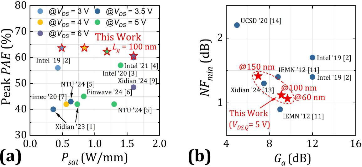
Figure 3: Benchmark of power and noise performance of devices with reported GaN-on-Si HEMTs at 26–30GHz: (a) peak PAE versus Psat at low voltage (≤6V); (b) NFmin versus Ga.
Benchmarking against previous reports (Figure 3), the team claims record high efficiency, more than 60%, and state-of-the-art 1.1dB noise performance at 100nm, i.e.without extreme lateral scaling.
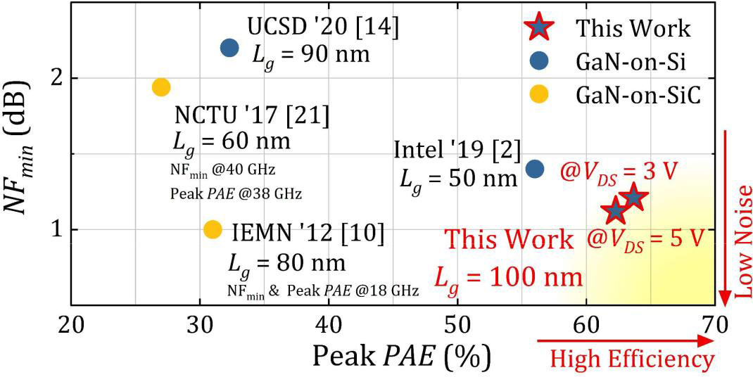
Figure 4: Benchmark of NFmin versus peak PAE for GaN HEMTs at ~30GHz, unless otherwise stated.
A further benchmark (Figure 4) shows the HEMTs to have high efficiency and low noise simultaneously compared with both GaN/Si and the more expensive GaN on silicon carbide (SiC) technology.
GaN-on-silicon HEMTs GaN Millimeter-wave 5G GaN MOCVD
https://doi.org/10.1109/LED.2026.3651778
https://www.everythingrf.com/community/5g-fr2-frequency-bands
The author Mike Cooke is a freelance technology journalist who has worked in the semiconductor and advanced technology sectors since 1997.


