News: Microelectronics
27July 2026
First experimental demonstration of S-band large-signal performance for GaN HBTs
A Chinese research team has achieved consecutive breakthroughs in gallium nitride (GaN) heterojunction bipolar transistors (HBTs), with results published in IEEE Electron Device Letters (IEEE EDL) in both 2025 and 2026. The 2026 paper was selected as an Editor’s Pick, marking a transition for GaN HBTs from frequency characterization to practical power application evaluation.
Due to their vertical current transport structure and the high critical electric field inherent to wide-bandgap materials, GaN-based HBTs offer significant theoretical advantages for high-power, high-frequency RF applications. However, compared to commercially established gallium arsenide (GaAs) HBTs and rapidly advancing GaN high-electron-mobility transistors (HEMTs), the RF performance of GaN HBTs has long been stagnant, with cut-off frequency (fT) and maximum oscillation frequency (fmax) previously limited to around 8GHz and 1.8GHz, respectively. The primary bottlenecks were twofold: the high resistivity of the p-type GaN base layer and surface damage from dry etching, which caused Schottky-like base contacts and high base resistance (RB), severely limiting fmax; and high emitter contact resistance (RE-M) in scaled devices, which increased collector charging time (τC) and limited fT.
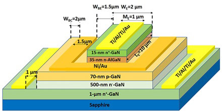
Figure 1: Schematic diagram of the GaN HBT with SAG n-AlGaN emitter.
In 2025, the team published a paper ‘AlGaN/GaN Heterojunction Bipolar Transistors With Record fT/fmax = 21.6/4.23GHz’ (L. Zhang et al, IEEE Electron Device Letters, 46(6), 912-915, 2025), marking the first time that GaN HBT frequencies were pushed into the S-band. This breakthrough was achieved through three key technological innovations. First, the team employed a selective-area epitaxial emitter technology, avoiding the base etching process and successfully achieving ohmic base contacts for the first time, with a specific contact resistivity of 3.23x10⁻³Ω cm2. Second, they introduced a heavily doped n+-GaN emitter cap layer, reducing the specific emitter contact resistivity to 1.35x10⁻⁷Ω cm2 and effectively lowering the collector charging time. Third, critical dimensions such as the base-emitter spacing were scaled down, further reducing parasitic resistances and capacitances. The resulting device demonstrated a record fT of 21.6GHz and fmax of 4.23GHz. The base-to-collector electron transit time was reduced to 6.9ps, only one-quarter of previously reported values. This device also achieved the highest recorded values for GaN HBTs on sapphire substrates: a saturated current density of 91.9kA/cm2, and a DC power density of 1.31MW/cm2.
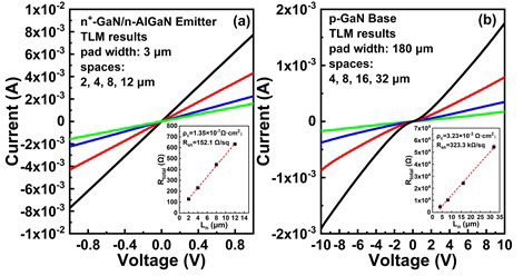
Figure 2: The I-V curves and resistance of the TLM structure on the regrown emitter layer and base layer.
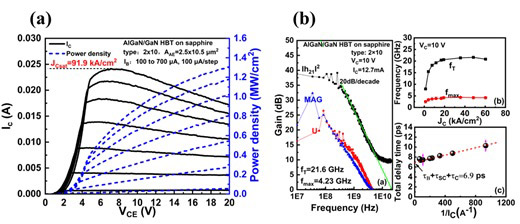
Figure 3: the AlGaN/GaN HBT with design AE = 2x10μm2: (a) common-emitter family curves; (b) the frequency performance and the fitted delay time.
In 2026, the team published a follow-up paper ‘Experimental Demonstration of S-Band Gallium Nitride Heterojunction Bipolar Transistors With Pout = 16.5kW/cm2’ (L. Zhang et al, IEEE Electron Device Letters, 47(7), 1306-1309, 2026), which was selected as an ‘Editor’s Pick’. This work further pushed the frequency and power records of GaN HBTs. Building on the 2025 results, the team adopted a high-aspect-ratio emitter design, increasing the emitter area to 3x80μm2 to reduce emitter contact resistance and on-resistance, thereby enhancing power output capability. Critically, the team systematically investigated the impact of the base-emitter spacing (WBE) on device performance. Reducing WBE from 2μm to 1μm resulted in a 67% increase in fmax, from 4.19GHz to a record 7.01GHz for GaN HBTs. Devices with WBE =2μm achieved a record fT of 30.5GHz, the highest ever reported for a GaN HBT. For power characterization, the team performed continuous-wave large-signal load-pull measurements in the S-band. At 2.4GHz and VCE = 10V, the scaled device demonstrated an output power density of 16.5kW/cm2. This is the first experimental demonstration of S-band large-signal performance for a GaN HBT, confirming the inherent high-power-density advantage of the vertical structure.
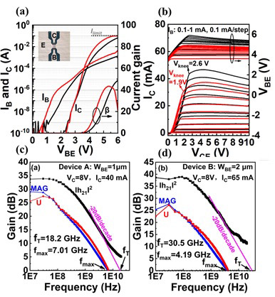
Figure 4: Measured characteristics of the GaN HBTs with different base-emitter spacing: (a) Gummel plot curves; (b) family curves; (c) and (d) frequency performances.
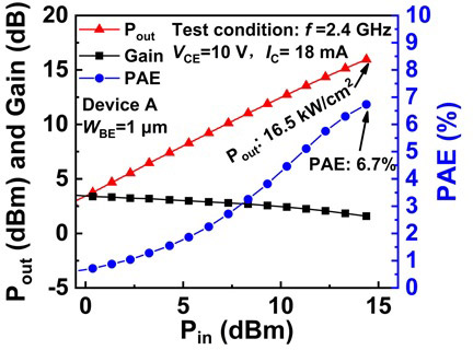
Figure 5: Large-signal performance of the GaN HBT.
Through the systematic adoption of selective-area epitaxial emitter technology, the introduction of a heavily doped cap layer, and the scaling of device dimensions, the team has systematically addressed the parasitic resistance bottlenecks that have long constrained GaN HBT RF performance. The team states that future work, including the use of SiC or GaN substrates for improved thermal management and further optimization of device dimensions and structure, holds promise for significantly enhancing power-added efficiency (PAE) and advancing the practical application of GaN HBTs in S-band power amplifiers.
Selective-area emitter for gallium nitride bipolar transistors
https://doi.org/10.1109/LED.2025.3558540