


News: LEDs
22 June 2026
Monolithic all-GaN 2T1C-μLED–photodetector integration
Two researchers at China’s Shandong University have reported monolithic integration (Figure 1) of all-gallium nitride (GaN) circuits consisting of 2 transistors (2T), 1 capacitor (1C), a micro-light-emitting diode (μLED) and a photodetector (PD) [Yipin Gao and Chao Liu, ACS Photonics, published online 22 May 2026].
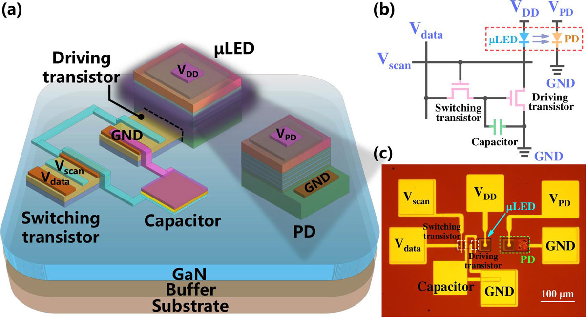
Figure 1: (a) Schematic, (b) equivalent circuit, and (c) microscope image of monolithically integrated all-GaN 2T1C-μLED–PDs.
Gao and Liu comment: “The integration of 2T1C architecture with μLEDs and PDs into the all-GaN pixel units unlocks several critical capabilities, which distinguish our work from prior GaN-based optoelectronic integrations. The integrated 2T1C-μLED–PDs feature an ultra-compact layout, with all functional components and their spacing in the micrometer range, avoiding extra optics and system volume. Each pixel unit potentially serves as a pixel-level optical transceiver. Additionally, the all-GaN pixel units theoretically support the convergence of micro-display and optical communication.”
The researchers see their approach as potentially leading to next-generation portable and wearable intelligent terminals: “During normal display operation, dedicated high-speed modulation signals can be superimposed on the data lines without disturbing the steady-state brightness. The 2T1C-μLEDs thus simultaneously act as optical transmitters and display pixels, while the near-coupled PDs receive incoming optical signals. This feature may transform the micro-displays into interactive platforms for smart wearable and portable electronics.”
The monolithic structure eliminates the problems associated with alternative transfer and bonding steps required for silicon CMOS-based and thin-film transistor micro-displays such as thermal mismatch, alignment inaccuracy, and parasitic degradation of system reliability and high-frequency performance.
Gao and Liu comment: “The monolithic integration scheme enables high-volume, precisely controllable fabrication of pixel units within a single GaN platform, which represents a simplified and technologically feasible path to future high-density arrays and display-sensing-communication integrated terminals.”
The 2T1C architecture is a core building block of active-matrix (AM) displays, allowing high brightness, enhanced grayscale control, and low power consumption over alternatives.
The researchers fabricated monolithic 2T1C-μLED–PD circuits containing two 20μm×20μm transistors, one 40μm×40μm μLED, and one 40μm×40μm PD (Figure 2). The LED-PD separation was 30μm.
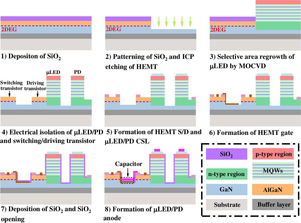
Figure 2: Fabrication processes of monolithically integrated 2T1C-μLED–PDs.
The high-electron-mobility transistor (HEMT) aluminium gallium nitride (AlGaN)/GaN layers were grown by metal-organic chemical vapor deposition (MOCVD) on 4-inch substrates. The μ-LED and PD multiple quantum well (MQW) and contact layer structures were fabricated by inductively coupled plasma (ICP) etching and MOCVD regrowth using a plasma-enhanced chemical vapor deposition (PECVD) silicon dioxide (SiO2) mask.
The electrical isolation of the μLED and PD was performed in ICP mesa etching. The SiO2 was removed by hydrofluoric wet etching, and then the transistor regions defined by ICP etching, along with exposing the n-GaN contact layer of the PD.
The n-type (cathode) PD and ohmic source/drain transistor metal contacts consisted of annealed titanium/aluminium/nickel/gold. Indium tin oxide (ITO) was used as a current-spreading layer on the p-contacts of the μLED and PD.
The titanium/platinum/gold gate electrodes were deposited after oxygen plasma treatment of the transistors. The bottom capacitor (1C) electrode was also formed from the gate metals. The devices were then covered with 600nm SiO2, which served for passivation and the capacitor dielectric.
The circuits were completed with deposition of titanium/nickel/gold stacks through the passivation forming the p-electrodes of the μLED and PD, and the top capacitor electrode.
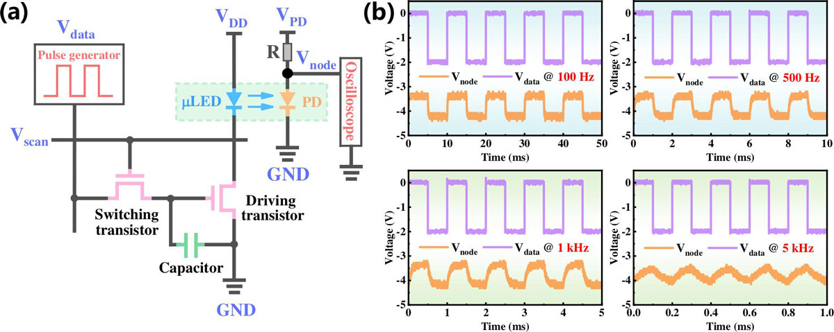
Figure 3: (a) Test circuit for (b) dynamic switching response measurements.
The dynamic switching response (Figure 3) is considered crucial for display refreshing and visible light communication (VLC) functionality. Gao and Liu comment: “Vnode exhibits a well-synchronized and clear response to the input Vdata signal at a frequency of 5kHz. The results confirm that the monolithically integrated μLEDs, pixel circuits, and PDs can seamlessly work together within the ultra-compact footprint, validating the basic functionalities of 2T1C-μLED–PDs for applications requiring simultaneous light emission and detection.”
μLED–photodetector integration GaN HEMT PECVD MOCVD
https://doi.org/10.1021/acsphotonics.6c00179
The author Mike Cooke is a freelance technology journalist who has worked in the semiconductor and advanced technology sectors since 1997.


