


News: Optoelectronics
24 June 2026
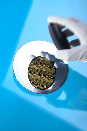
TNO and ASML join forces to scale European photonic chip manufacturing
The research institute TNO (the Netherlands Organization for Applied Scientific Research in Delft) and equipment provider Advanced Semiconductor Materials Lithography (ASML) of Veldhoven, The Netherlands have announced a new partnership that aims to strengthen the European semiconductor ecosystem through the development and industrialization of photonic chips. The collaboration focuses on the utilization of TNO’s new Photonic Chip Pilot Line currently under construction at the High Tech Campus in Eindhoven.
Scaling integrated photonics
By aligning their technical expertise, the parties aim to enable scalable, high-volume manufacturing of photonic chips through lithography, process control, and metrology solutions. The partnership involves a phased approach where ASML utilizes lithography equipment, including DUV and i-line scanners, within the pilot line facility. This shared R&D environment facilitates technical workshops and joint innovation activities, allowing ASML to leverage TNO’s infrastructure for internal development and customer demonstrations.
 Strengthening European high-tech
Once operational, the fab will facilitate full-scale manufacturing of indium phosphide (InP) photonic chips at a 6-inch wafer scale. Beyond physical manufacturing, the research ecosystem is already primed to leverage these advances. TNO, Eindhoven University of Technology, and the University of Twente are working together within the jointly founded Photonic Integration Technology Centre (PITC) to turn innovative designs into real-world applications. This new structured collaboration with ASML is designed to improve operational performance and ensure that Europe remains a global leader in the rapidly evolving integrated photonics landscape.
“This partnership with ASML reinforces our commitment to building European unicorns in the semiconductor landscape,” says Arnaud de Jong, managing director TNO High Tech Industry. “By combining our R&D capabilities with world-class equipment, we are creating a unique pilot-line environment that will benefit the entire industry,” he adds.
“Scaling photonic chip technology requires a seamless transition from cutting-edge research to high-volume manufacturing,” notes Stanislas Baron, senior VP at ASML. “By integrating our lithography systems into TNO’s pilot line, we are bridging that gap,” he adds. “This collaboration gives us the ideal environment to optimize our processes for integrated photonics, ultimately accelerating the time-to-market for this transformative technology.”


