


News: LEDs
22 June 2026
Purifying red InGaN micro-LED spectra
Researchers in China have effectively eliminated dual-peak emissions in red indium gallium nitride (InGaN) multiple quantum well (MQW) micro-LEDs [Chunyu Liu et al, Appl. Phys. Lett., v128, p191103, 2026].
The team from Xiamen University, Future Display Institute of Xiamen, and Southern University of Science and Technology, studied the compositional pulling effect (CPE) in metal-organic chemical vapor deposition (MOCVD) of InGaN QWs, allowing the fabrication of LEDs with a single, symmetric red peak up to a current density of 100A/cm2.
The CPE is caused by compressive strain in high-indium-content InGaN layers on GaN and results in vertical composition inhomogeneity along the growth direction. The researchers found that reducing the growth temperature for the lower QWs, increasing the indium content, effectively compensated for the CPE.
The researchers comment: “This approach provides a practical remedy toward high-color-purity, high-efficiency InGaN red micro-LEDs, offering a strong potential for III–nitride-based full-color micro-LED displays. By tuning the growth temperature for each individual QW, it should be possible to achieve a homogeneous indium composition in all QWs.”
Although traditionally InGaN has much reduced external quantum efficiency (EQE) in the red spectral range, it has attractive properties for the micro-LEDs needed for micro-displays over the more conventional red-emitting semiconductor combination of aluminium gallium indium phosphide (AlGaInP). In particular, AlGaInP LEDs have EQEs typically below 1% when their dimensions scale below 5μm, compared with 20% for mm-scale mini red LED EQEs of the same materials.
Red InGaN LEDs should also be easier to integrate with existing green and blue InGaN LEDs to create monolithic micro-LED full-color displays for virtual/augmented reality (VR/AR) systems.
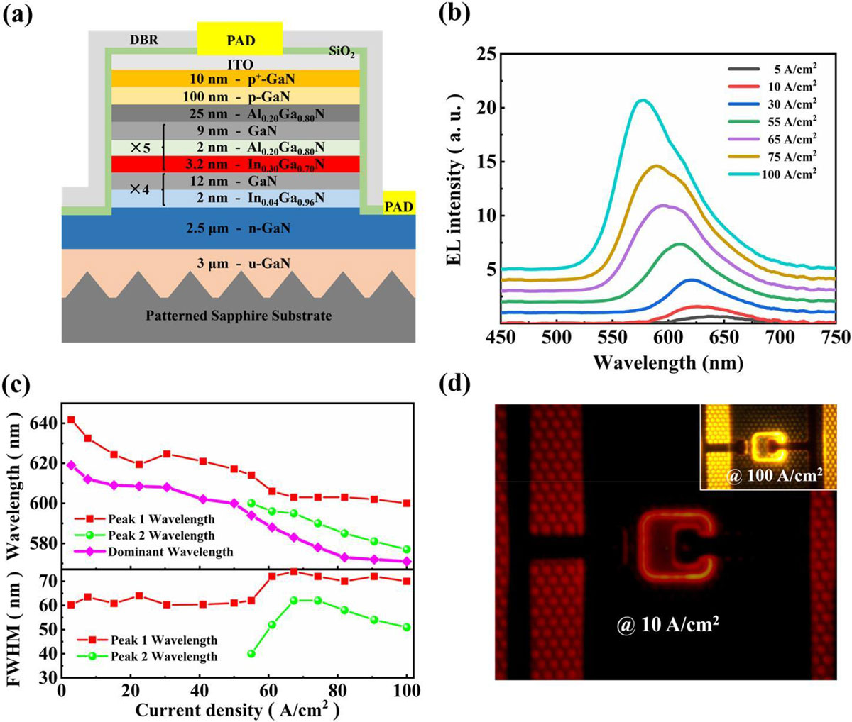
Figure 1: (a) InGaN-based red LED structure profile. (b) EL spectra of 15μm×15μm micro-LED (Sample A) under 5–100A/cm2 current density. (c) Peak wavelength and FWHM extracted from Gaussian fit. (d) Optical microscopy images of Sample A at 10A/cm2 and 100A/cm2. Dark center due to contact and DBR.
The researchers prepared LED structures using MOCVD on patterned sapphire (Figure 1). The structure included a 4-period (x4) InGaN pre-strain layer and a 5-period (x5) MQW active region with 35% indium content InGaN aimed at red emission. The MQW was subjected to two growth strategies: in sample A the wells were grown at the same temperature; in sample B the first two wells were grown at 5°C lower. The sample B recipe was aimed at compensating for the CPE.
Fabricated micro-LEDs included an indium tin oxide (ITO) transparent conducting layer for current spreading, a silicon dioxide (SiO2) passivation layer, and a titanium/silicon-dioxide distributed Bragg reflector (DBR) to enhance light extraction from the substrate side.
The single growth temperature of sample A results in the micro-LED emitting a single peak up to 55A/cm2, after which a shoulder appears in the spectrum, indicating a second peak. Between 5A/cm2 and 55A/cm2 the peak shifts to shorter wavelengths from 635nm to 611nm, respectively. The researchers comment on the blueshift: “This is caused by the screening of the piezo-electric field and the band-filling effect that are commonly observed in long-wavelength InGaN LEDs.”
At higher current injection, the second peak appeared around 580nm (600nm at 55A/cm2). The team comments: “The enhanced short-wavelength emission at high injection indicates preferential carrier population in the bottom QWs, which is attributed to improved hole injection and their relatively higher radiative recombination efficiency associated with lower indium composition.”
Both peaks blue-shift at higher injection, decreasing to 600nm and 577nm at 100A/cm2. The team comments: “The dual-wavelength emission under high current injections severely deteriorates the color purity, limiting their applications for full-color displays.”
The researchers used cross-sectional cathodoluminescence (CL) hyperspectral analysis to study the responses of the individual QWs. The lower wells were found to emit at shorter wavelengths: around 597nm in the upper QWs and 570nm in the lower. The method did not allow resolution into individual QW responses. The team explains: “This gradual red-shift toward the p-side suggests a compositional variation of indium within the InGaN MQWs, where the upper QWs show a higher indium composition. The observed spectral variation is intrinsic to the sample and not an artifact of the extraction region.”
Thus, the shift to longer wavelengths on the p-side “tends to support that the increased indium incorporation from the bottom to the top of the MQWs, supposed to be caused by CPE, is the true reason for the dual EL peaks.”
Energy-dispersive x-ray (EDX) analysis (Figure 2) showed a 12% difference in indium content between the bottom and top wells of sample A.
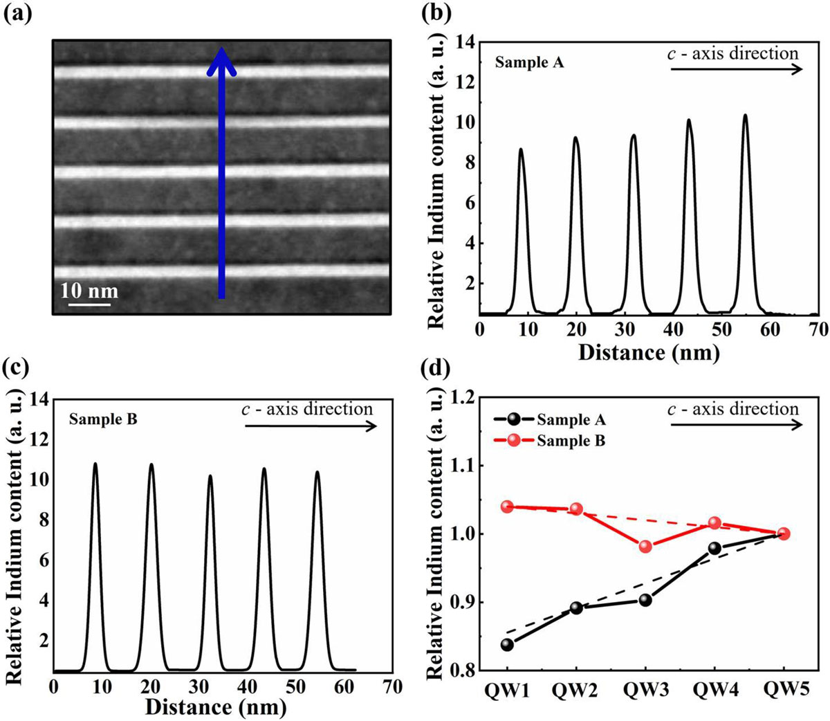
Figure 2: (a) Scanning transmission electron microscope (STEM) image of sample A’s MQW. (b) EDX analysis of sample A MQW indium composition. (c) Sample B EDX analysis. (d) Indium composition distributions for samples A and B. Dashed lines: guides for the eye. Indium compositions normalized to last QW for each sample.
The researchers comment: “Dislocations can be newly generated during the red InGaN QW growth due to the high indium composition, leading to partial relaxation of strain. As a result, the indium incorporation is enhanced for the QW growth afterward, causing the compositional variation as we observed here. In addition, the enhanced polarization field associated with increased indium compositions intensifies the quantum-confined Stark effect (QCSE), leading to a further red-shifted emission from the upper QWs, whereas the lower indium compositions in the bottom QWs lead to the short-wavelength emission peak.”
The researchers based the reduction of the growth temperature of the first two wells by 5°C on previous work suggesting that a 1°C reduction corresponds to about 6nm of wavelength in InGaN. The sample B EDX results showed a more constrained compositional variation of 4%.
The spectral analysis of sample B micro-LED showed a single peak with stable full-width at half-maximum (FWHM) of 45.6nm in the range 50–100A/cm2 (Figure 3). By contrast, sample A LEDs had FWHMs increasing from 64.0nm to 73.7nm over the same injection range. The peak external quantum efficiency reached 7.9% at 5.2A/cm2 for B, while A only managed just over half that.
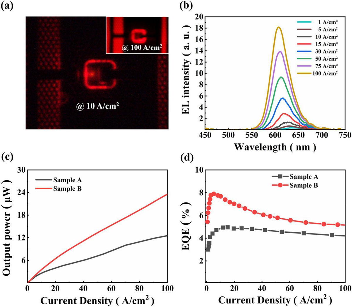
Figure 3: and (d) comparison of light output power and EQEs between A and B micro-LEDs.
The wavelength at peak EQE for LED B was 619nm, reducing to 612nm at 100A/cm2. The wavelength shift between 1A/cm2 and 100A/cm2 was 24nm, “which is not large compared to results from other groups”, the team adds.
Red InGaN micro-LED InGaN MOCVD
https://doi.org/10.1063/5.0324915
The author Mike Cooke is a freelance technology journalist who has worked in the semiconductor and advanced technology sectors since 1997.


