


News: Optoelectronics
9 March 2026
Induced fit Ga- semiconductor growth
Shandong University in China reports on an “induced fit growth method” for creating gallium-based semiconductor thin films on amorphous gallium oxide (GaOx) on various substrates [Zixu Sa et al, Light: Science Applications, v15, p103, 2026]. The researchers see the method as being analogous to how enzymes enable the correct folding of polypeptide (amino acid) chains into functional proteins rather than into an amorphous mess.
The team, which also included researchers from City University of Hong Kong and Kyushu University, Japan, believe the technique could enabling Ga-based semiconductor optoelectronics on a variety of substrates, such as flexible mica and rigid glass.
The resulting thin-film material was deployed into thin-film transistor (TFTs) and photodetectors. The TFTs had synapse-like responses, raising the potential for deployment in artificial machine intelligence, neuromorphic computing and Internet of Things. The photodetectors had omnidirectional sensing capability, and an imaging array was demonstrated.
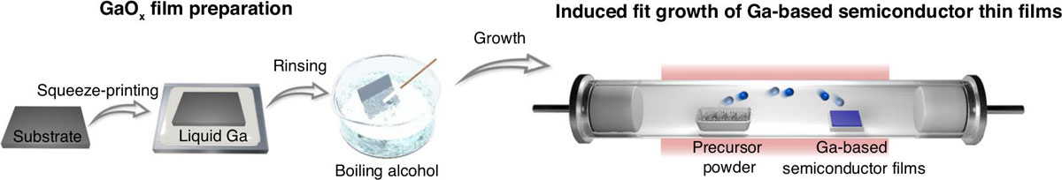
Figure 1: Induced fit growth scheme for Ga-based semiconductor films.
The amorphous GaOx film was prepared using the liquid metal van der Waals exfoliation method (Figure 1). This involved “gently” pressing a substrate (silicon or silicon dioxide, in this case) vertically onto heated liquid Ga on glass. When lifted away in air an amorphous GaOx formed on the substrate. Residual liquid Ga droplets were removed by rinsing with boiling alcohol.
The induced fit growth was carried out in a dual-zone horizontal tube furnace. The sources were Ga-based semiconductor powders placed in the upstream zone. The GaOx substrate/template was placed downstream. The upstream zone was heated to temperatures in the range 750–850°C while downstream temperatures were 400–550°C, dependent on the desired semiconductor film. The pressure was 7mTorr. The carrier gas was nitrogen. The carrier flow was maintained during the cool-down to room temperature.
The main work concentrated on gallium antimonide (GaSb) films, but the researchers have successfully used the same process to deposit gallium compounded with selenium (GaSe), arsenic (GaAs), and in GaSb/GaAs alloy form (GaAsSb).
The researchers note that they were unable to grow similar Ga semiconductor films on spin-coated GaOx. They believe that this was due to the absence of Ga excess regions in the spin-coated GaOx. These free metal Ga regions in the exfoliated GaOx allow the induced fit growth of island crystal structures (Figure 2).
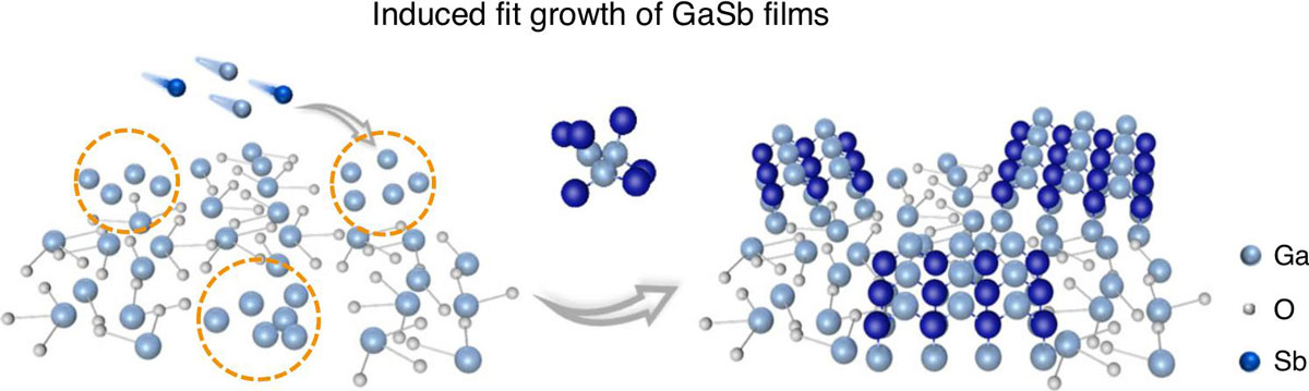
Figure 2: Atomic-level diagram of induced fit growth method.
The researchers comment: “With the prolonged growth duration, the film gradually becomes compact and uniform. In brief, the as-proposed induced fit growth method paves the way for the growth of multi-functional semiconductor thin films on arbitrary substrates.”
From a more conventional crystal growth perspective (e.g. metal-organic chemical vapor deposition) this seems analogous to epitaxial layer overgrowth (ELO), but on a much smaller scale. In ELO ‘small’ regions are opened in a mask on the crystal substrate to be used as seeds for low-defect crystal growth. For induced fit growth, the seed is Ga metal to which the group V atoms can attach in an ordered manner, seeding the crystal islands (islets?).
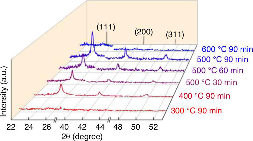
Figure 3: X-ray diffraction (XRD) scans of GaSb films prepared at different growth temperatures and durations.
The researchers found that the strongest XRD peaks were seen in GaSb material grown at 500°C for 90 minutes (Figure 3). XRD analysis is often deployed to assess the crystallinity of materials. The researchers also used other materials analysis techniques such as atomic force microscopy (AFM), optical and electron microscopy, and energy-dispersive x-ray spectroscopy (EDS).
The optoelectronic properties of the thin films were explored by fabricating thin-film and synaptic transistors, along with photodetectors.
The back-gated TFTs were p-type devices with a maximum hole mobility of 0.25cm2/V-s for a GaSb channel grown for 90 minutes at 500°C.
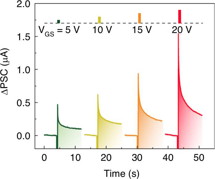
Figure 4: Synaptic plasticity triggered by positive gate (VGS) pulses.
The TFTs demonstrated ‘synaptic’ effects, based on charge-trapping behavior, which is often not desired in other electronic applications. Under 100ms gate pulses of various intensity, a ‘post-synaptic current (PSC)’ was triggered (Figure 4).
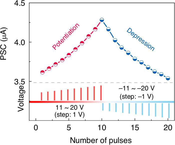
Figure 5: Long-term plasticity (LTP) and depression (LTD) realized by applying 20 VGS pulses at 100ms intervals.
The behavior of synapses changes according to previous conditions, which usually come in the form of repeated electrical pulses. The GaSb devices mimicked such behavior (Figure 5). Other synapse-like behavior the team was able to realize included paired pulse facilitation (PPF), spike rate-dependent plasticity (SRDP), and spike timing-dependent plasticity (STDP).
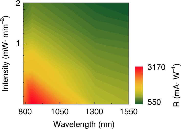
Figure 6: Wavelength-dependent broadband photodetection by as-prepared GaSb films under 0.57mW/mm2 laser intensity.
The photodetection between 800nm and 1550nm infrared showed responsivity (R) and and detectivity (D*) levels as high as 3170mA/W and 5.3x10⁹ Jones, respectively (Figure 6).
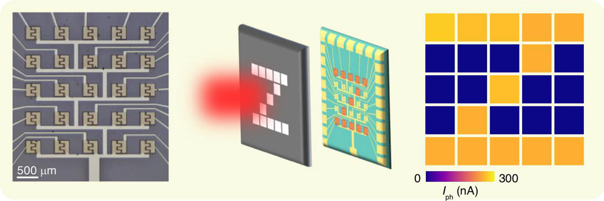
Figure 7: Near infrared (NIR) photodetection 5x5-pixel imaging array.
A 5x5-pixel imaging array maintained its performance for a period of up 60 days (Figure 7).
Amorphous gallium oxide TFTs ELO
https://doi.org/10.1038/s41377-025-02096-2
The author Mike Cooke is a freelance technology journalist who has worked in the semiconductor and advanced technology sectors since 1997.


