


News: Microelectronics
21 May 2026
Sidewall gating of GaN HEMTs
Researchers with three US universities have reported on gallium nitride (GaN) sidewall-gated high-electron-mobility transistors (SG-HEMTs) [Rian Guan et al., IEEE Electron Device Letters, published online 30 March, 2026]. The work at Pennsylvania State University, University of Illinois Urbana Champaign, and University of California Santa Barbara, was supported in part by the US Office of Naval Research.
The device structure (Figure 1) aimed at high threshold voltage, high breakdown, and low gate capacitance.
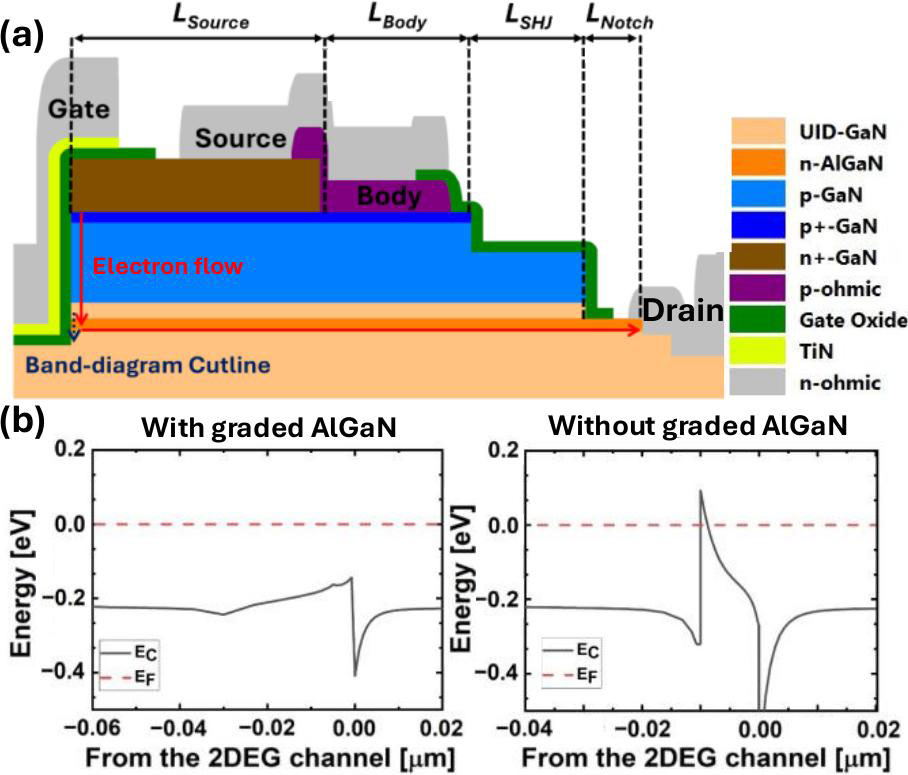
Figure 1: (a) AlGaN/GaN SG-HEMT cross section. (b) Simulated band-diagram along vertical channel under 4V positive gate potential.
The researchers explain the operation: “To turn the transistor on, a positive bias is applied to the sidewall gate, inducing a vertical inversion channel at the interface between the gate oxide and the p-GaN sidewall. Electrons flow vertically from the n+-GaN, through the inversion channel and the AlGaN barrier, reaching the two-dimensional electron gas (2DEG), then flow laterally through the 2DEG channel to the drain electrode. The AlGaN barrier needs to be n-type doped and compositionally graded to reduce the barrier for electron flow from the inversion channel to the 2DEG.”
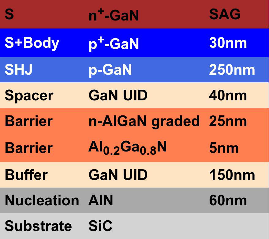
Figure 2: Epitaxial heterostructure used for SG-HEMT.
The device material was grown on silicon carbide (SiC) by metal-organic chemical vapor deposition (Figure 2). The resulting 2DEG in the GaN just below the AlGaN barrier had 4.5x10¹²/cm2 carrier density, and 749Ω/□ sheet resistance, according to contactless Hall measurement. The top n+-GaN source (S) contact was applied using selective-area growth (SAG).
The material was etched by inductively coupled plasma (ICP). The mesa isolation also included implantation of aluminium ions. The gate oxide was a bilayer of 7nm AlN and 13nm of aluminium oxide (Al2O3). The gate metal was plasma-enhanced atomic layer deposition (PEALD) titanium nitride (TiN). The p- and n-ohmic metals were palladium/gold and Ti/Al, respectively. The gate breakdown voltage of the gate dielectric layers was estimated at 16V.
The devices were 100μm wide. The length of the super-heterojunction (SHJ) region was varied, but the other dimensions for the region from the drain were 3μm notch, 6μm body, and 11μm source. There was some electrostatic gating over the region up to the notch, making the effective channel length around 17μm, which reduced the saturation current of the devices to around 70mA/mm for 10V gate potential.
At room temperature the threshold varied between 3.5V for up-sweeps and 4V for down-sweeps. This hysteresis was blamed on “the high density of donor-like trap states on the etched p-GaN surface”. The hysteresis widened at 200°C with the up-threshold dropping further to 2.7V, than for the down- point at 3.8V.
The researchers comment: “The increase of hysteresis and negative shift of VTH can be attributed to the increase of trap state capture and emission rates of slow donor-like trap states with temperature. This phenomenon raises concerns about gate hysteresis and reliability for long-term usage.”
Higher turn-on voltages give more tolerance against false turn-ons when switching high voltages at higher speeds.
The off-state leakage was sub nA/mm at 0.1V drain bias (VDS). This increased to sub μA/mm when the bias was raised to 5V, but stayed at this level on increasing the bias to 10V.
The team explains: “This leakage current is due to vertical reverse leakage of the bipolar n+-GaN/p-GaN/2DEG junction, which can be reduced by minimizing the length of n+-GaN. As the VDS increases, the PN junction in the SHJ region becomes reverse-biased, depleting the 2DEG. Once fully depleted, the additional VDS will drop in the SHJ region rather than vertical channel, causing no further increase of the vertical leakage current.”
The off-state breakdown voltage (BV) behavior was significantly improved by H2 plasma treatment during device fabrication (Figure 3). Without treatment the breakdown occurred around 350V for all lengths of SHJ.
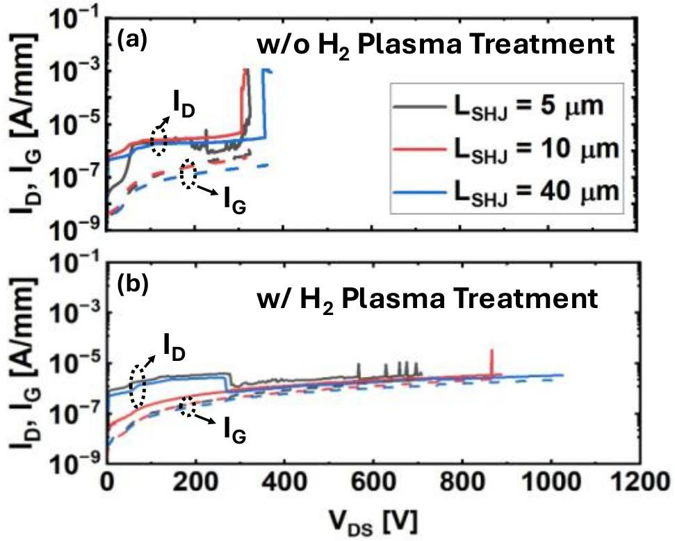
Figure 3: Off-state current–voltage (I–V) characteristics with different LSHJ (a) before and (b) after H2 plasma treatment.
The researchers comment: “Longer LSHJ didn’t result in expected BV increase. This is attributed to charge imbalance in the SHJ of this particular sample. To meet ideal charge balance between donors and acceptors in the SHJ region, the remaining p-GaN thickness should be 100nm, However, variation in GaN etch rate during device processing resulted in a remaining p-GaN thickness of 150nm, therefore an acceptor-rich condition. This caused the electric field crowd at the edge of the p-GaN near the drain contact.”
The treatment succeeded in reducing the imbalance, resulting in much higher breakdowns: 700V, 900V and 1050V, respectively, for SHJ lengths of 5μm, 10μm and 40μm. The researchers expect further increases in breakdown for optimized charge balance structures.
Dynamic switching resulted in less than 40% degradation of on-resistance measured 1ms after the off-on transition.
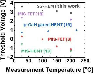
The researchers also compared their threshold voltages with other reports (Figure 4). Across the temperature range up to 200°C, their devices achieved the highest threshold values.
Figure 4: Comparison of threshold voltage at elevated temperature with other experimental GaN transistor structures.
A further advantage was an “extremely low” gate capacitance (Cgd), less than 200fF, as needed for low-loss hard switching.
https://doi.org/10.1109/LED.2026.3678286
The author Mike Cooke is a freelance technology journalist who has worked in the semiconductor and advanced technology sectors since 1997.


