


News: LEDs
21 May 2026
Nanopillar GaN LED arrays for VR and AR
China’s Institute of Semiconductors and University of Chinese Academy of Sciences have reported progress in fabricating high-resolution light-emitting diode (LED) display arrays with up to 500x150 pixels with 6336pixels/inch (PPI) density [Le Zhang et al, Jpn. J. Appl. Phys., v65, p070904, 2026]. The researchers also report passive-matrix addressing of a smaller 6x6 array.
The researchers comment: “This work provides a viable technical reference for the scalable fabrication of ultra-high-resolution micro/nano-LED display devices.”
The team believes that, with reduction of the pixel pitch, an increase to more than 10,000PPI is possible. Such densities are needed for near-eye virtual-reality and augmented-reality (VR/AR) applications.
The researchers comment: “After decades of development and iteration, the self-emissive micro-LEDs have attracted widespread research interest due to their distinctive advantages. Compared to liquid-crystal displays and organic LEDs, GaN-based micro-LEDs offer significant advantages such as high contrast, high brightness, long lifetime, and a wide color gamut, making them strong contenders for next-generation display technology.”
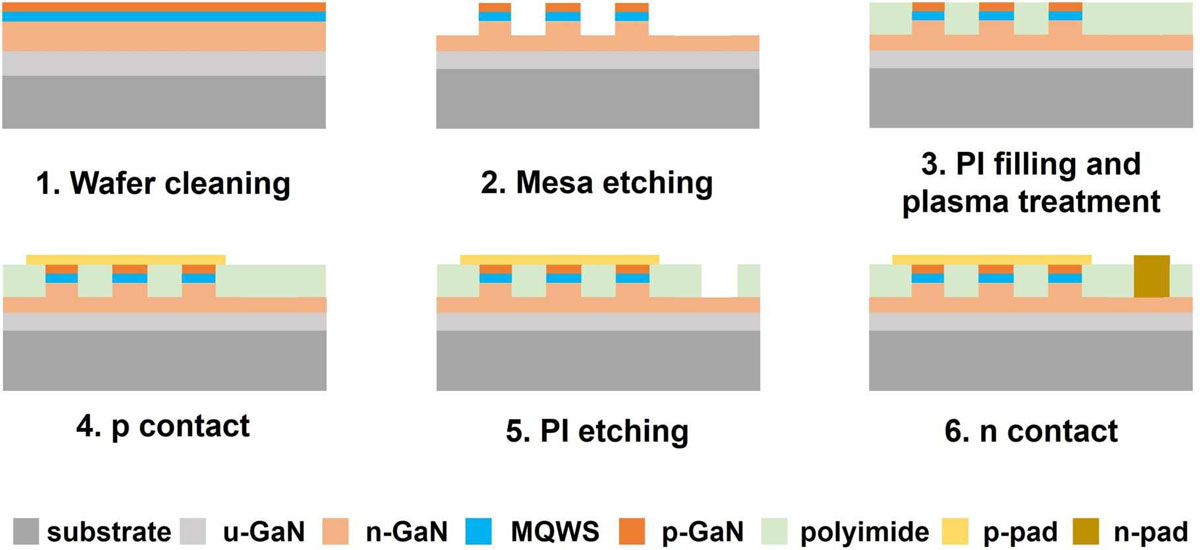
Figure 1: Process flow.
The material for the devices (Figure 1) was prepared on gallium nitride (GaN)/sapphire templates, using metal-organic chemical vapor deposition. The blue-emitting layer consisted of three quantum wells of indium gallium nitride (InGaN) separated by GaN barrier layers. Aluminium gallium nitride was used in an electron-blocking layer (EBL) between the wells and p-contact.
The layers were relatively thin: 300nm and 90nm for the n- and p-contacts, respectively, and 10nm for the EBL.
The researchers explain: “The fabrication of such thin LED structures is primarily motivated by two factors: first, it effectively reduces the etching depth, which can mitigate sidewall damage induced by dry etching. A shallower etch depth corresponds to shorter etching time, allowing for the use of thinner and more easily removable photoresist as an etch mask, thereby enabling better control over dimensions and morphology during etching. Second, reducing the nanopillar height (aspect ratio) facilitates the insulating layer planarization process, alleviating difficulties in electrode interconnection, thereby lowering process complexity and minimizing lithographic deviations.”
Optical lithography was used to pattern the nanopillars, etched to a depth of 300nm using inductively coupled plasma (ICP). The sidewall damage from the ICP process was repaired using tetramethylammonium hydroxide (TMAH) solution treatment.
ICP tends to result in rough sidewalls, which offer opportunities for parasitic current flows, reducing LED efficiency. The TMAH smooths the nanopillars, enhancing device effectiveness. Such reduction of sidewall damage is particularly critical as device sizes scale down, increasing surface area/volume ratios.
The researchers comment: “TMAH, a hydroxyl-based chemical, reacts minimally with the c-plane of GaN but etches its sidewalls (m-plane or a-plane) effectively. It is also known to reduce the density of surface states, which act as non-radiative recombination centers, and is therefore commonly used in III-nitride device processing.”
The pillars were 800nm diameter, placed in arrays at 4μm pitch in orthogonal directions, giving 6336pixels/inch (PPI) density.
The space between the nanopillars was filled with polyimide (PI) transparent insulator. The n- and p-metal contacts were titanium/aluminium and nickel/gold, respectively. The tops of the nanopillars were exposed in an etch-back of the PI material before the p-metal deposition. The etch-back also reduced 76.8nm nanopillar height variations down to 12.3nm. A deeper etch was needed to access the n-contact layer for n-metal deposition.
Another advantage of the nanopillar structure with steep sidewalls is to suppress sidewall light emission, reducing optical crosstalk between pixels.
The electroluminescence peak blue-shift of a parallel-connected 500x150 nanopillar array as the injected current increased from 10mA to 100mA (Figure 2) was 5.1nm: “This blue-shift originates primarily from the quantum-confined Stark effect (QCSE) and band-filling effects,” the team explains. In the current density range 30–80A/cm2 (10–30mA), the shift was only 2.2nm, compared with 2.8nm for thin-film LEDs fabricated on the same material.
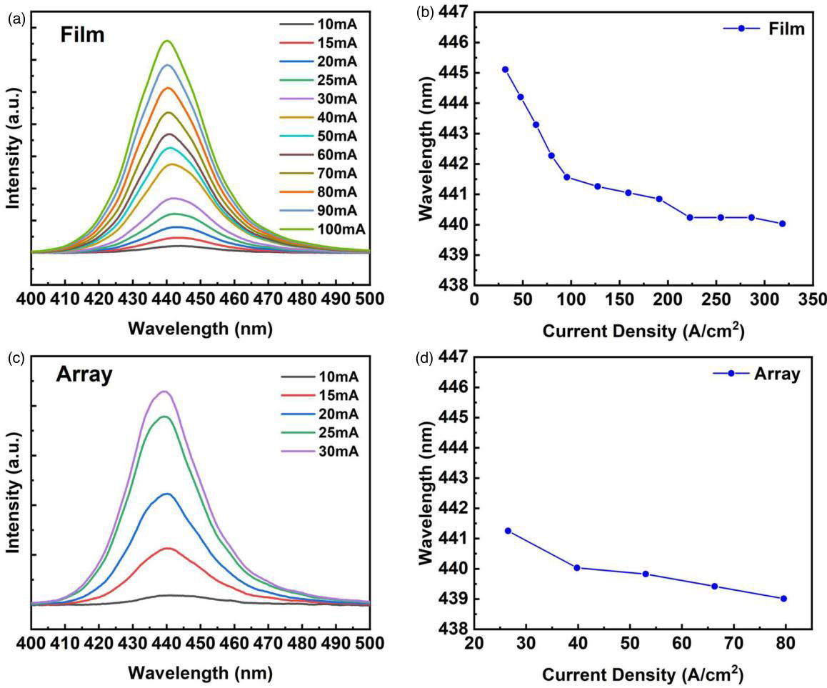
Figure 2: (a) (c) Electroluminescence spectra of thin-film and nanopillar array LEDs, respectively, versus injection current at room temperature. (b) (d) Corresponding peak wavelength positions.
The researchers comment: “This reduction is attributed to the effective relaxation of strain in the nanopillar structure, which mitigates the internal QCSE. Furthermore, at the same current level, the emission peak of the nanopillar array is noticeably blue-shifted compared to that of the thin film.”
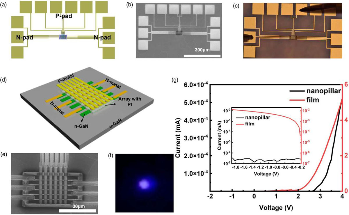
Figure 3: (a) Passive-matrix mask design for 6x6 array. Scanning electron (SEM) (b) and optical microscope (c) images. (d) Schematic illustration of passive matrix driving setup. (e) Locally magnified SEM image at device center. (f) Optical micrograph of pixel emission activated by probe control. (g) Current–voltage characteristics of thin-film LED and nanopillar LEDs. Inset: logarithm current versus voltages for samples. The right-hand scales refer to higher (around four orders of magnitude) current levels of larger thin-film devices.
The researchers also explored the potential for passive-matrix (PM) driving of the individual pixels (Figure 3). Orthogonal row x column contact lines enable current to flow through the separate LEDs. The current density of blue-emitting nanopillar LED is around 100A/cm2.
https://doi.org/10.35848/1347-4065/ae574a
The author Mike Cooke is a freelance technology journalist who has worked in the semiconductor and advanced technology sectors since 1997.


