
News: LEDs
10 November 2026
Staera emerges from stealth with $4.6m in pre-seed funding
Staera Semiconductor of San Francisco, CA, USA has emerged from stealth with a technology that builds optical data links directly into silicon chips. It targets the problem that now limits how fast and how large AI systems can grow: moving data between chips. Formerly New Silicon Corp (NSC), the company has raised $4.6m in pre-seed funding, led by Openspace Capital with participation from SGInnovate, Black Kite Capital, 28 Holdings, In Group, and Decimus Technologies.
AI chips now compute faster than copper wiring can feed them. Copper’s electrical performance falls a thousandfold between 1mm and 1m (the distances that connect chips, boards and racks). Staera’s first product, Lightwire, replaces those copper links with light generated inside the chip itself, made with the same process and on the same wafer as the chip’s circuits.
Transition from copper wiring to optical links
AI’s next limit is moving data, not computing it. The International Energy Agency expects data-center electricity use to more than double, from 415 terawatt-hours in 2024 to about 945 terawatt-hours by 2030, and copper wiring cannot carry more data further without burning more power. That is pushing the industry's biggest buyers toward light: Nvidia, which said in 2025 it would “stay with copper for as long as [they] can”, now plans to use both copper and optics in its AI systems. Lightwire says it is built for that mix.
Light built in, not bolted on
Most optical links currently are separate parts, lasers or LEDs made elsewhere and attached next to the chip. Staera fabricates the light source and every other part of a complete optical link inside commercial silicon wafers, making Lightwire the first and only optical interconnect built fully into the chip itself, it is claimed. The links are designed to be made in existing fabs and add no extra size, heat or power. Staera has built gallium nitride (GaN) LEDs into silicon chips in commercial foundries since 2016 with processes that now run at 98-99% yield.
“AI’s bottleneck is no longer how fast chips compute, but how fast and far they can move data,” says CEO Dr Andrew Kim. “Copper performance plummets over the millimeter-to-meter distances that matter most in AI accelerators, and bolt-on optics add power and complexity. We build the light into the chip, the entire optical link inside a chip, so the connection gets smaller, cooler and faster with each generation. This funding takes Lightwire from the lab to customers, and the Staera name marks that move.”
Lightwire is built inside the bridge or interposer chip that already connects processors and memory in existing AI hardware, so it works with existing packaging. Staera designs it to move data using less than a tenth of the energy of today’s best optical links. Moving 24 terabytes of data per second would consume less than 50W with Lightwire, compared with nearly a kilowatt using co-packaged optics.
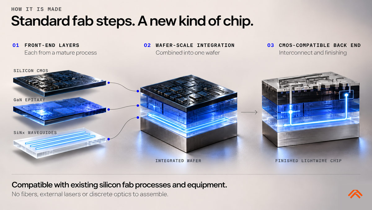
Picture: Staera makes its chips using standard fab steps, combining silicon CMOS, GaN and waveguide layers on a single wafer. (Image: Staera)
Details of Lightwire are as follows:
- 4-8Gbps per link, with more than 600 links per millimeter of chip edge;
- designed for under 0.2pJ/bit, against about 5pJ/bit for co-packaged optics;
- more than 100x the performance of electrical links across the millimeter-to-meter range;
- reaches beyond 50mm, against 2mm for UCIe-A die-to-die links;
- Lightwire-based HBM designed to exceed 24TB/s, against 2.8TB/s per HBM4 stack today.
From lab to customers
The pre-seed round marks Staera’s shift from research to commercial product. The company will use the funding to advance its technology, expand its team into the USA, and deepen engagement with its customers and supply chain partners, targeting commercial release in 2030.
“Staera is addressing one of AI infrastructure’s most urgent challenges: moving vast amounts of data between chips without a corresponding rise in power, heat and complexity,” comments Openspace Capital’s co-founder Hian Goh. “Its ability to build optical links directly into silicon offers a compelling path to faster, more efficient, and more scalable AI systems. We backed Staera because of the strength of its technology, the depth of its team and its potential to define a new category in semiconductor connectivity.”
In May, Staera won the 3rd ECTC Start-up Competition at the IEEE Electronic Components and Technology Conference (ECTC), themed ‘The Light Age: Strategic Investment in Photonics to Power the Next Computing Era’. The same month, it was runner-up at the 2026 Lam Capital Venture Competition, run by Lam Research in Fremont, CA, USA.