

News: LEDs
19 November 2026
Barrier engineering for green micro-LEDs
Xiamen University and Future Display Institute of Xiamen, China, have reported a systematic investigation on quantum barrier (QB) design for green micro-LEDs aimed at active-matrix micro-displays [Chunyu Liu et al, ACS Photonics, online 21 October 2026)
Such display applications require high performance at low current injection. The electrons and holes need to be brought together in such devices with the maximum utilization of the injected carriers to produce photons.
The researchers believe their work establishes “a unified active-region design principle in which QB engineering controls the number of effectively radiative quantum wells, enabling multiple quantum wells (MQWs) to be optimized for high-efficiency III–nitride micro-LEDs operating under display-relevant low-current conditions.”
The team’s devices achieved impressive wall-plug efficiency (WPE) and external quantum efficiency (EQE) up to 52.4% and 48.1%, respectively.
The researchers comment: “Increasing QB thickness suppresses inter-well hole transport, promotes carrier redistribution toward the radiatively active QWs near the p-side, and improves electron−hole overlap. As a result, radiative recombination becomes dominant at substantially lower injection levels.”
Holes are particularly difficult to redistribute away from the p-side of the device since they have low mobility, related to their higher effective mass relative to electrons.
The researchers grew the material for the test LEDs by metal-organic chemical vapor deposition (MOCVD) (Figure 1). The precursors for the quantum well (QW) region were trimethyl-indium (TMIn) and triethyl-gallium (TEGa), along with ammonia (NH3). TMGa was also used in other layers in the structure.
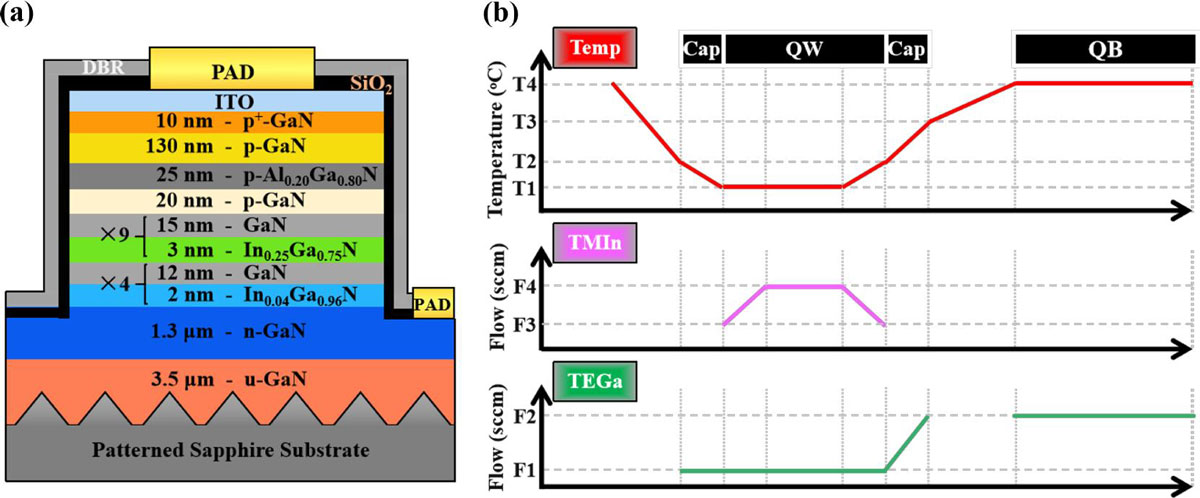
Figure 1: (a) Schematic InGaN-based green LED structure. (b) Optimized epitaxial growth conditions.
The QW region consisted of up to nine pairs of InGaN/GaN. The structure also included a 4x(InGaN/GaN) pre-strain region before the QWs, and a p-type aluminium gallium nitride (p-AlGaN) electron-blocking layer (EBL).
The researchers designed the QWs to have a trapezoidal band profile, “to enhance carrier confinement and promote radiative recombination”. The higher temperature used to grow the quantum barriers was arranged “to enhance adatom migration and ensure high crystalline quality”.
The QB thickness was varied between 10nm and 25nm in 5nm steps, giving four samples — A, B, C and D, respectively. The team also explored reducing the number of QWs to 7, 5 or 3 with 25nm QB thickness.
The fabricated LEDs included an indium tin oxide (ITO) current-spreading layer, silicon dioxide (SiO2) sidewall passivation, and a distributed Bragg reflector (DBR). The 13μm×26μm test chips were mounted in a flipped configuration with light emerging through the sapphire substrate.
The researchers performed a variety of x-ray analyses on the material samples such as high-resolution x-ray diffraction (HRXRD), reciprocal space mapping (RSM), and x-ray reflectivity (XRR) measurements.
The team summarizes: “Overall, the combined HRXRD, RSM and XRR analyses demonstrate that increasing the QB thickness improves the structural uniformity and heterointerface abruptness of the MQW active region without inducing strain relaxation or significant degradation in crystalline quality. The improved structural quality of MQWs is expected to promote carrier confinement and transport.”
The electroluminescence measurements for champion (i.e. best) devices based on materials A–D showed green (500–565nm) wavelength peaks around 531–532nm (Figure 2). The researchers comment: “To our knowledge, the achieved performance is among the highest reported for green InGaN-based micro-LEDs.”
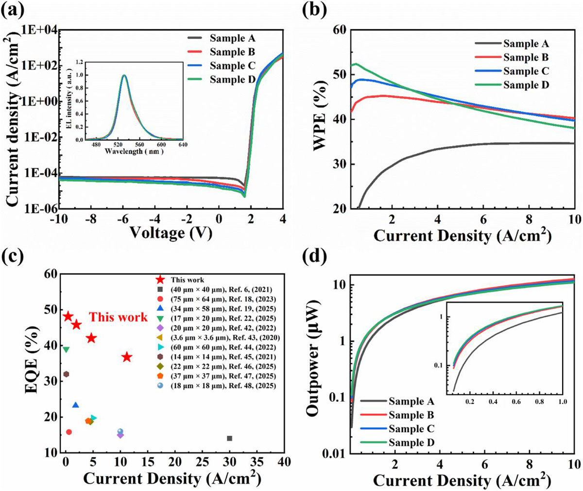
Figure 2: Current density versus voltage for samples AD. Inset: corresponding normalized electroluminescence spectra at 5.8A/cm2. (b) WPE versus– current density for champion devices. (c) EQE versus current density for reported green micro-LEDs compared with LED based on sample D. (d) Light output power versus current density.
The researchers comment: “Although thicker QBs may slightly modify the strain distribution and polarization field across the MQWs, the associated variation in QCSE is expected to be substantially screened under moderate current injection because of carrier-induced screening of the internal electric field. Consequently, the negligible wavelength shift indicates that QB engineering primarily modifies carrier transport and recombination rather than the emission band structure.”
Wall-plug efficiency (WPE) and external quantum efficiency (EQE) measurements showed LEDs based on sample D to have the highest performance at low current injection. The WPE reached 52.4% at 0.42A/cm2 injection. At this current, the EQE was 48.1%.
The researchers explain: “The slightly higher WPE than EQE is consistent with the low forward voltage operation, where the photon energy exceeds the electrical energy consumed per carrier.”
The rising WPE performance in the plotted range for sample A is attributed to higher non-radiative recombination through the Shockley–Read–Hall mechanism, indicating a higher defect density. Other groups have obtained better low-current green micro-LED performance with 10nm QBs. The researchers attribute this to differences in active-region designs and operating-current regimes.
The team comments: “Because all samples exhibit nearly identical emission wavelengths, the enhancement in WPE is primarily attributed to improved carrier transport and recombination within the MQW active region rather than changes in the emission band structure.”
At higher injection currents, above 5A/cm2 the power performance of LEDs based on sample D falls below that of those using the other samples — presumably due to “the onset of additional efficiency-limiting mechanisms under high-injection conditions”, the team says.
Reducing the number of QWs to five was found to increase the average (rather than ‘champion’) peak WPE of sample D LEDs from 39.6% (at 0.93A/cm2) to 47.8% (0.31A/cm2). Reducing to three QWs did not achieve a further increase in WPE, but trended down to 44.3% at 0.55A/cm2. The averages were over 160 devices per wafer.
The researchers comment: “These results suggest that MQW optimization for low-current micro-LED operation requires balancing carrier utilization efficiency and effective recombination volume.”
On the basis of theoretical considerations, the researchers believe “the optimum MQW design is governed not by the maximum number of MQWs, but by matching the geometrical MQW structure to the effective radiative recombination volume established by QB-controlled carrier redistribution.”
Green micro-LEDs GaN InGaN MOCVD
https://doi.org/10.1021/acsphotonics.6c01862
The author Mike Cooke is a freelance technology journalist who has worked in the semiconductor and advanced technology sectors since 1997.