

News: Microelectronics
1 October 2026
Intrinsic polarization superjunctions
École Polytechnique Fédérale de Lausanne (EPFL) in Switzerland has reported on the benefits of intrinsic polarization superjunctions (iPSJs) for gallium nitride (GaN)-based lateral electronic devices [Luca Mazzone et al, Nat. Electron., published online 28 August 2026].
The researchers see the structure on silicon (Si) as being a potential route to monolithic integration of high-voltage devices on the same wafer for integrated power circuits. The iPSJ structure simultaneously provides low resistance and high breakdown voltages with robust operation up 125°C. The use of silicon could enable economies of scale on large wafers of 8-inch diameter and more.
The iPSJ concept uses spontaneous and piezoelectric charge polarization fields to induce matching two-dimensional electron and hole gases in a charge-balanced superjunction without intentional doping. This allows the creation of more uniform electric fields in drift regions, delaying the peak electric field from going into critical breakdown. Alternately, higher breakdown performance allows shorter drift regions to be used, reducing on-resistance.
The epitaxial material for the iPSJ devices consisted of GaN/AlGaN/GaN layers on 6-inch silicon grown by metal-organic chemical vapor deposition (Figure 1). The layers were undoped except for a 50nm p-GaN cap layer designed to enable ohmic contact. For Schottky barrier diodes (SBDs), the buffer/u-GaN/u-AlGaN/u-GaN sequence was 7μm/400nm/30nm/300nm. The AlGaN alloy used a 35% aluminium content. Both AlGaN-GaN interfaces included 1nm AlN spacers.
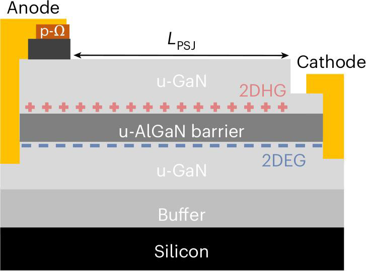
Figure 1: iPSJ Schottky barrier diode (SBD).
The charge-matched material contained two-dimensional electron (2DEG) and hole (2DHG) gases. The 2DEG had a sheet carrier density of 1.03×10¹³/cm2 and 1,832cm2/V-s, according to Hall measurements on van der Pauw structures. The corresponding figures for the 2DHG were 1.05×10¹³/cm2 and 12cm2/V-s, respectively. The much lower 2DHG mobility meant that its conduction was minimal.
The SBD device performance was compared with two variants using the same material. One variant removed the upper u-GaN material down to a residual thickness of 15nm, giving a charge-mismatched device. The other variant retained the p-GaN layer over the thick u-GaN layer in the drift region. The 100%-mismatched device structure had no detectable 2DHG and the electron carrier density increased to 1.27×10¹³/cm2. In the device with p-GaN cap the electron and hole densities were 14% mismatched in the opposite direction: 0.97×10¹³/cm2 2DEG and 1.12×10¹³/cm2 2DHG, respectively.
SBDs with a 25μm drift region (LPSJ) demonstrated turn-on voltages of 0.75V and specific on-resistance (RON,sp) of 4.7mΩ-cm2. The variant devices had similar performance in the low-voltage region.
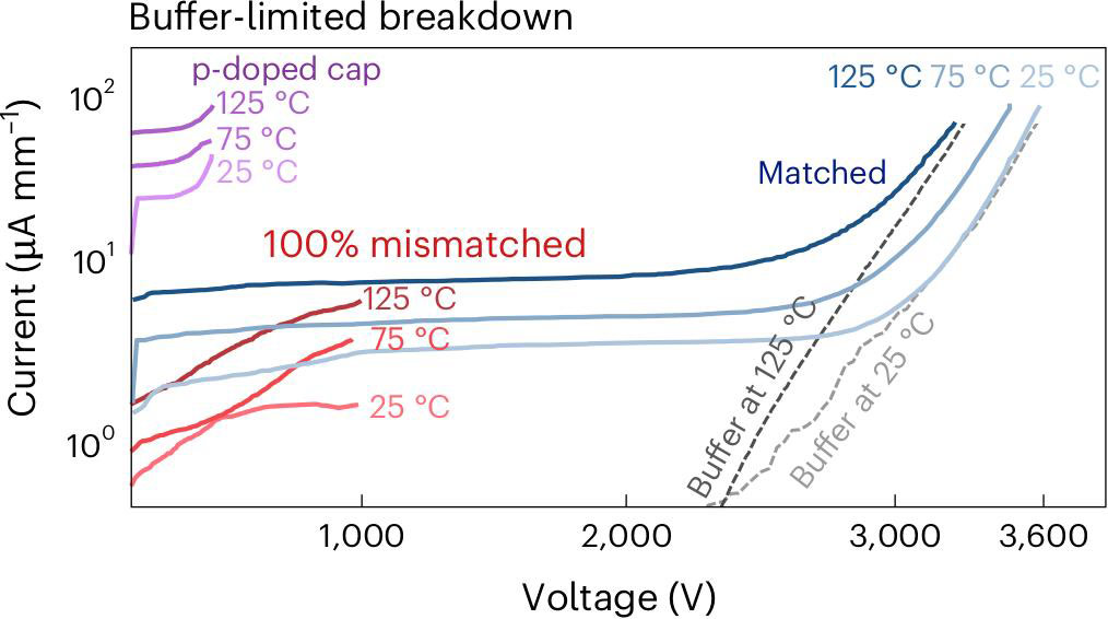
Figure 2: OFF-state characteristics at different temperatures (25°C, 75°C and 125°C) for all diode types (p-doped cap, mismatched and matched), with the same LPSJ of 25μm.
The charge-matched iPSJ SBD maintained an OFF-state, less than 100μA/mm, under reverse bias up to 3.6kV (Figure 2). At 3.9kV the device sustained a current flow of 0.95mA/mm without breaking down catastrophically.
The team reports: “A nearly flat leakage current was observed up to 3.1kV, beyond which buffer leakage dominated.”
The charge-mismatched device only managed 1kV before breakdown. The current leakage of this SBD steadily increased under reverse bias.
The researchers comment: “This degradation originates from the stronger dependence of the peak electric field on reverse voltage due to net fixed charges, leading to premature catastrophic breakdown. The absence of holes in the thin-cap device also lowers the leakage current.”
The p-cap device suffered catastrophic breakdown at 342V and 7-fold higher leakage.
The iPSJ SBD was also more thermally robust over temperatures up to 125°C. The researchers comment: “Unlike doped SJs, the carrier densities in electron and hole gases are set by polarization and remain stable for a large temperature range. In charge-matched diodes, leakage current increases moderately with temperature — consistent with thermionic emission and trap-assisted tunneling — whereas breakdown voltages (VBR) stay above 3.3kV up to 125°C, limited only by the GaN-on-Si buffer breakdown.”
The charge-matched device was able to sustain 17 voltage sweeps up to 3.3kV with negligible variation in behavior. “This repeatability is a key advantage of iPSJ, translating into more robust and reliable devices without the overdesign margins commonly required for GaN HEMTs,” the team comments.
The dynamic on-resistance was tested by ‘hard switching’ from an OFF-state maintained for 1s to a 3V ON-state for 1ms. The charge-matched devices were capable of switching from a 3kV OFF-state with negligible effect on the ON-resistance.
The u-GaN cap layer was found to effectively passivate surface trap degradation effects found in non-matched devices. In addition, the p-Ω contact mitigated the impact of residual traps in the buffer onto dynamic on-resistance and breakdown.
The researchers comment: “In particular, all results were obtained on cost-effective GaN-on-Si substrates, which typically exhibit larger trap densities and lower buffer-limited breakdown voltages compared with silicon carbide (SiC), sapphire or bulk GaN. Therefore, substantially higher voltages are expected by demonstrating iPSJs on these other substrates.”
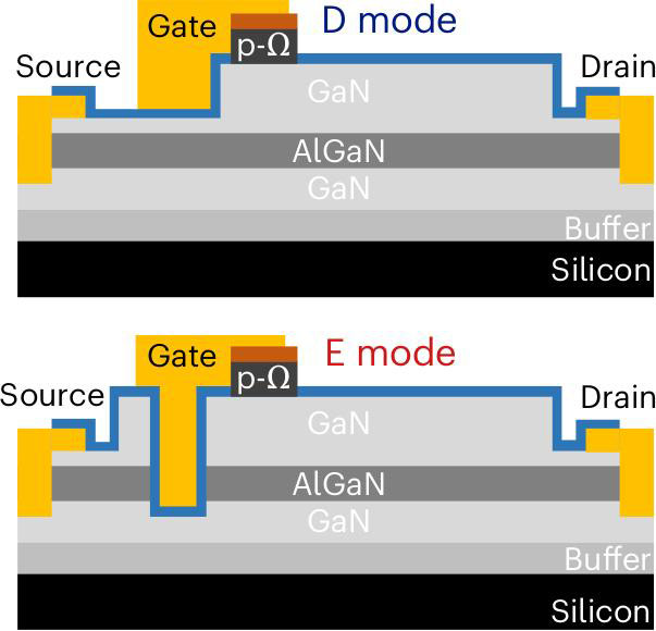
Figure 3: D- and E-mode lateral transistor structure schemes.
The researchers also fabricated lateral depletion- (D-, normally-on at 0V gate) and enhancement-mode (E-, normally-off) transistors using the iPSJ structure in the drift region (Figure 3). The u-GaN cap layer was 160nm. The devices avoided the use of complicated field-plate (FP) structures to massage the electric field into a more uniform profile. E-mode devices are often preferred for reduced power consumption and fail-safety operation characteristics.
The team comments: “By using a sufficiently thick u-GaN cap layer, charge-balanced 2DEG and 2DHG are induced, resulting in a charge-neutral drift region. A hybrid gate architecture is then introduced: a p-Ω region provides dynamic hole injection during turn-ON, analogous to a gate-injection transistor device, and efficient hole extraction during turn-OFF, thereby preserving charge balance during switching. The remaining gate metal directly modulates the 2DEG channel. A gate formed on the cap layer yields a normally-ON (D-mode) device, whereas a normally-OFF (E-mode) device is realized by recessing both cap layer and barrier beneath the gate to suppress the 2DEG, followed by the deposition of silicon dioxide (SiO2) and gate metal to form a metal−oxide−semiconductor (MOS) structure.”
Table 1: Performance of D- and E-mode iPSJ transistors.
Transistor |
Threshold (VTH) | RON,sp | VBR |
| D-mode | −7V | 6.3mΩ-cm2 | 3.5kV |
| E-mode | +0.67V | 11.1mΩ-cm2 | 3.4kV |
The transistors achieved ON/OFF ratios around five orders of magnitude, along with low on-resistance and high breakdown capability (Table 1). The researchers suggest lower on-resistance could come with use of heterostructures with lower sheet resistance or by using multi-channel heterostructures.
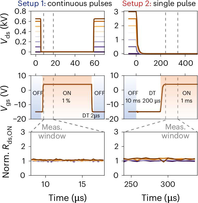
Figure 4: Time-resolved waveforms of Vds, Vgs and normalized ON-state resistance (Norm. Rds,ON) of the D-mode transistor with 25μm LPSJ, measured with continuous-pulse and single-pulse setups.
The dynamic on-resistance capability of the D-mode device was found to closely match that of the static condition (Figure 4).
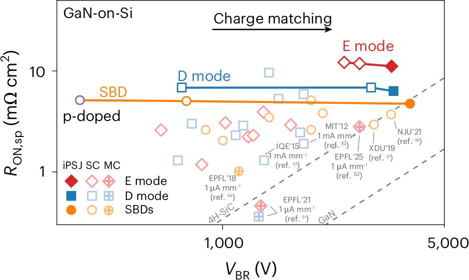
Figure 5: RON,sp versus VBR benchmarks of iPSJ devices against state-of-the-art lateral GaN-on-Si transistors and diodes with single- (SC) and multi- (MC) structures.
The researchers also compared their results with previous works (Figure 5). The team comments: “iPSJs achieved state-of-the-art performance among single-channel devices reported in the literature, and the highest VBR among all GaN-on-Si devices, surpassing conventional transistors and diodes that rely on additional FPs to mitigate electric-field crowding. In iPSJ devices, the breakdown voltage is governed solely by the charge-matching condition in the access region, and no FPs were used.”
Intrinsic polarization superjunctions GaN GaN-on-Si
https://doi.org/10.1038/s41928-026-01691-4
The author Mike Cooke is a freelance technology journalist who has worked in the semiconductor and advanced technology sectors since 1997.