

News: Microelectronics
22 October 2026
Thermal benefit of GaN-on-W power
Researchers from University of Bristol in the UK and Ferdinand-Braun-Institut (FBH) in Germany propose the use of tungsten substrates for gallium nitride (GaN) power devices for improved thermal performance at lower cost [Pharyanshu Kachhawa et al, Appl. Phys. Lett., p129, v133507 2026].
GaN devices are being deployed in a number of high-power switching applications due to its superior material properties. However, low-cost growth substrates such as sapphire or silicon present challenges for high performance. GaN-on-silicon tends to have high defect densities, due to lattice mismatching, that impact performance. Sapphire has a smaller mismatch, but high thermal resistance to heat dissipation. Low thermal resistance is vital to high-power switching, which can generate large amounts of heat.
The team reports: “We have demonstrated effective thermal management for GaN p–n power diodes grown on sapphire substrates (low-cost compared to bulk GaN substrates) by transferring the GaN membranes to high-thermal-conductivity tungsten metal substrates. A 3.1-fold reduction in device thermal resistance is demonstrated over the devices prior to the sapphire substrate transfer, attributed to the high thermal conductivity of the tungsten substrate and close to the ideal GaN-on-GaN case.”
The researchers used a process previously developed by FBH and Austria-based EV Group. The use of tungsten was favored over copper, another thermally conductive metal, as a compromise between electrical conductivity, thermal conductivity, commercial availability, and thermomechanical compatibility with GaN. The team comments: “Although Cu has higher thermal conductivity, its much larger thermal expansion coefficient relative to GaN would be expected to introduce larger residual stresses during cooling from the bonding temperature and during thermal cycling. This increases the risk of membrane bowing, cracking, or delamination.”
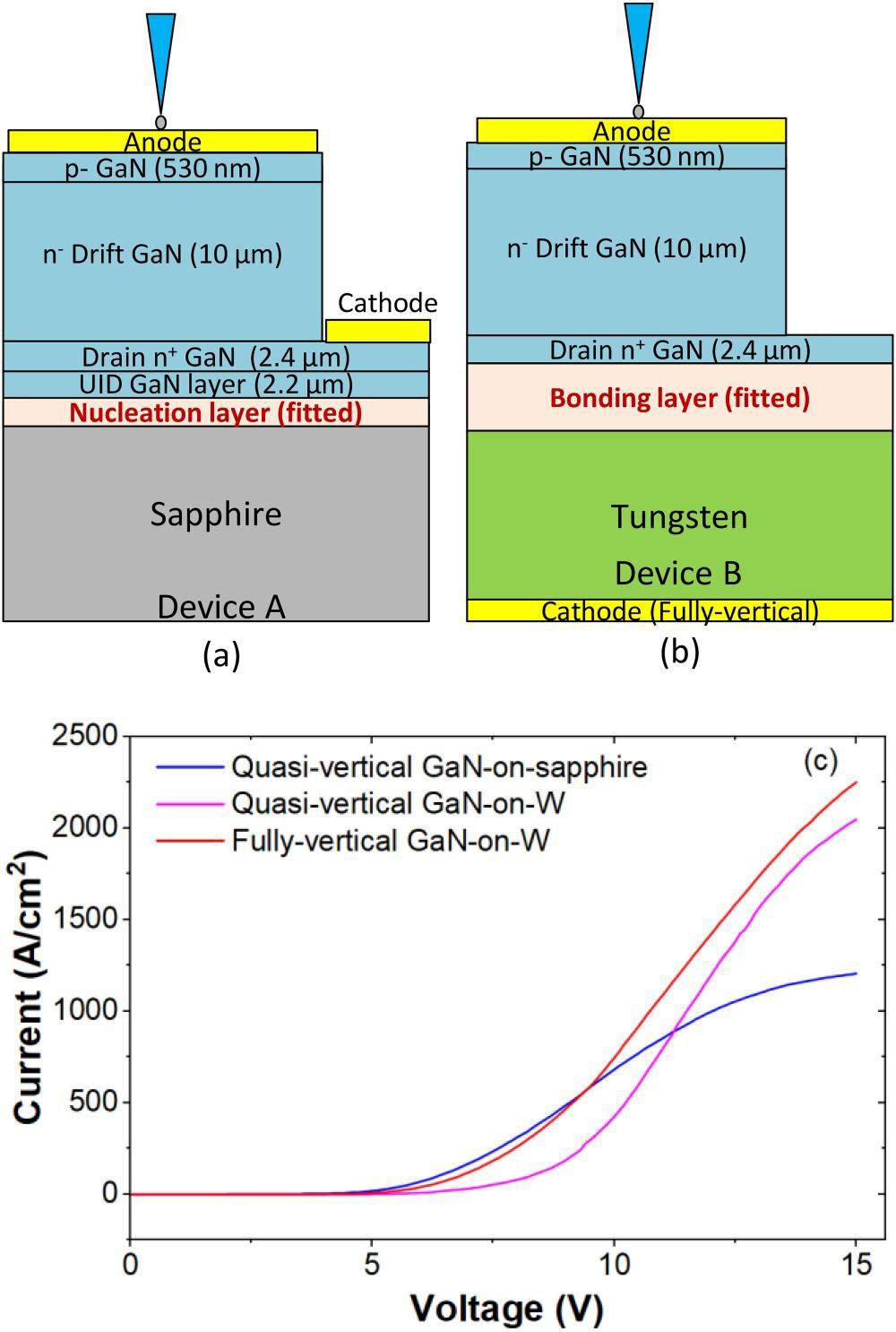
Figure 1: Device schematics for (a) quasi-vertical GaN-on-sapphire, (b) fully vertical GaN-on-W p–n diodes (tungsten substrate used as cathode), and (c) forward-bias electrical characteristics.
The GaN epitaxial material was grown by metal-organic chemical vapor deposition on sapphire and fabricated into diodes (Figure 1). The devices included a 300nm silicon nitride passivation layer.
Transfer to tungsten was accomplished by laser lift-off (LLO), removing the sapphire, and transient liquid phase (TLP) bonding to tungsten with 8μm ohmic contact metals, silver and tin.
Diodes on sapphire are usually restricted to a quasi-vertical format, with the cathode contact made to the buried n-type layers. This is due to the electrically insulating nature of the sapphire substrate. With transfer to electrically conducting tungsten, the cathode contact can be made through the carrier substrate, giving a fully vertical current flow path, which reduces electrical series resistance.
The fully vertical diode on tungsten allowed higher current flow after turn-on, compared with quasi-vertical devices on tungsten or sapphire.
The quasi-vertical diodes on tungsten showed higher forward current than on sapphire. The researchers attribute this to the improved thermal environment provided by the tungsten substrate, reducing self-heating-induced current degradation at high bias.
The devices were unoptimized research demonstrators for the GaN-on-W transfer platform. This resulted in less than ideal diode performance, such as the high and slow turn-on voltages, due to “contact and process-related series resistance contributions, particularly associated with the p-GaN anode contact and access regions.”
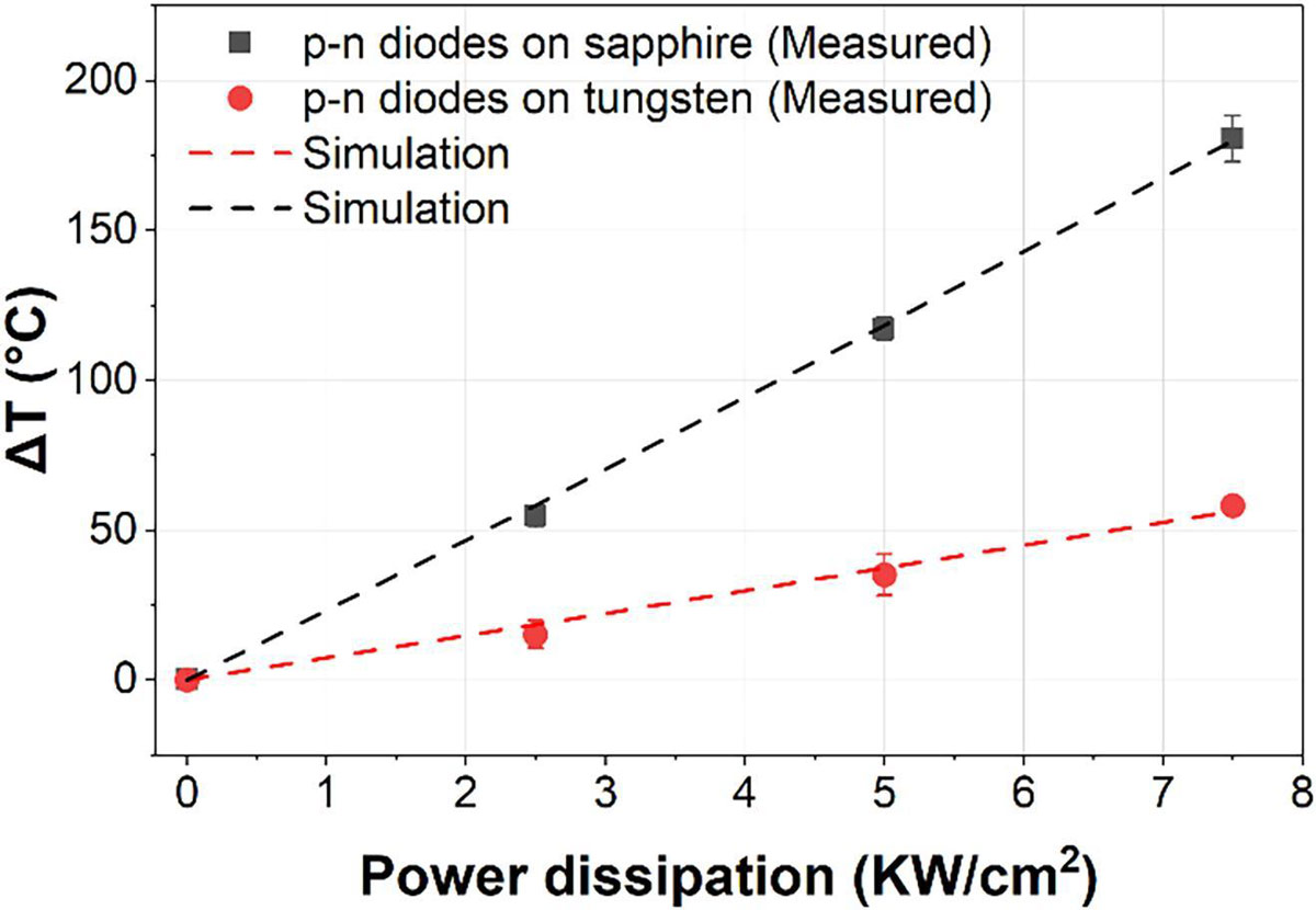
Figure 2: Measured Raman thermography temperature rise versus power dissipation. Dashed lines show results of finite-element simulations.
The focus of the reported research was rather to quantify the thermal benefit of substrate transfer to tungsten. The team used Raman nanoparticle thermometry to gauge the temperatures of the devices operated on a 22°C thermoelectric stage (Figure 2). The nanoparticles were around 50nm diameter, consisting of titanium dioxide (TiO2). Sonicated nanoparticles in ethanol were drop cast onto the diodes at 80°C, evaporating the ethanol. Variations in the 143/cm Raman signal of TiO2 allow the temperature variations to be calculated.
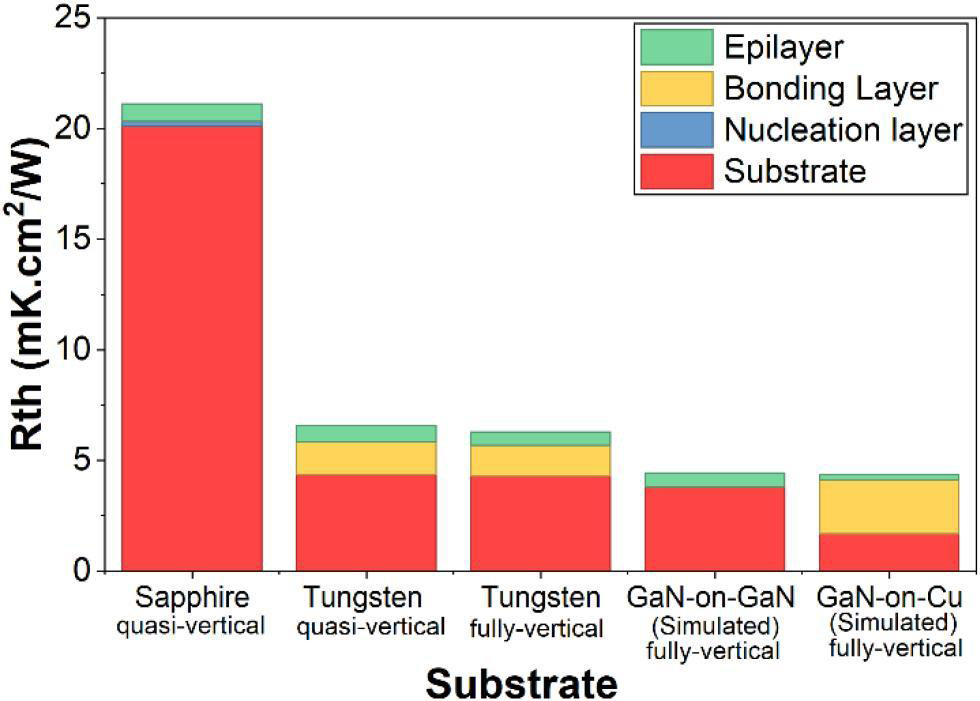
Figure 3: Device thermal resistance (Rth) contributions for different diode types, based on measurements and simulation.
The diodes on tungsten showed much reduced resistance to power dissipation, enabling a lower junction temperature and hence improved performance (Figure 3). Although simulations suggest somewhat better performance from GaN-on-GaN and GaN-on-copper (Cu), the team comments: “While the GaN-on-Cu device shows Rth comparable to the homoepitaxial GaN-on-GaN structure, we note that the large CTE mismatch between Cu and GaN would lead to high thermomechanical instability under the thermal cycling encountered during real power device operation. The GaN-on-W platform, therefore, provides similarly strong thermal performance for high-power-density applications compared to Cu, with the added benefit of improved thermomechanical compatibility with GaN.”
GaN p–n power diodes GaN Sapphire substrates MOCVD
https://doi.org/10.1063/5.0345342
The author Mike Cooke is a freelance technology journalist who has worked in the semiconductor and advanced technology sectors since 1997.