

News: LEDs
13 October 2026
InGaN amber nano-LED with 10% external quantum efficiency
Researchers based in China and Malaysia report conventional nano-scale amber light-emitting diodes (LEDs) based on indium gallium nitride (InGaN) with 10% peak external quantum efficiency (EQE) [Yunpeng Ge et al, Appl. Phys. Lett., v129, p091104, 2026].
The team from Xiamen University, Future Display Institute of Xiamen, University of Malaya, and Nanjing University, comments: “In contrast to aluminium gallium indium phosphide (AlGaInP) devices, which undergo a severe efficiency collapse under aggressive down-scaling, the present result shows that the InGaN platform can preserve high efficiency in the nanoscale regime. This benchmark indicates that strong carrier localization and size-enhanced light extraction allow top-down InGaN red nano-LEDs to extend efficient electroluminescence into the sub-1μm regime. Unlike nanowire-based architectures, this performance is achieved in a planar geometry that remains compatible with scalable wafer-level processing.”
The researchers see efficient long-wavelength nano-LEDs as being essential for ultrahigh-density monolithic RGB micro-displays, as used in augmented/virtual-reality systems (AR/VR). Efficiency is often negatively impacted in smaller devices, typically due to non-radiative carrier recombination and current leakage at sidewalls. The ratio of sidewall area/device volume is inversely proportional to size.
The epitaxial structure (Figure 1) was grown on patterned sapphire substrate (PSS) by metal-organic chemical vapor deposition (MOCVD). The structure included an In0.05Ga0.95N/GaN superlattice (SL). The light-emitting active region consisted of 5 In0.3Ga0.7N multiple quantum wells (MQWs) capped with AlGaN, and separated by GaN quantum barriers (QBs). An electron-blocking layer (EBL) was provided by Al0.2Ga0.8N.
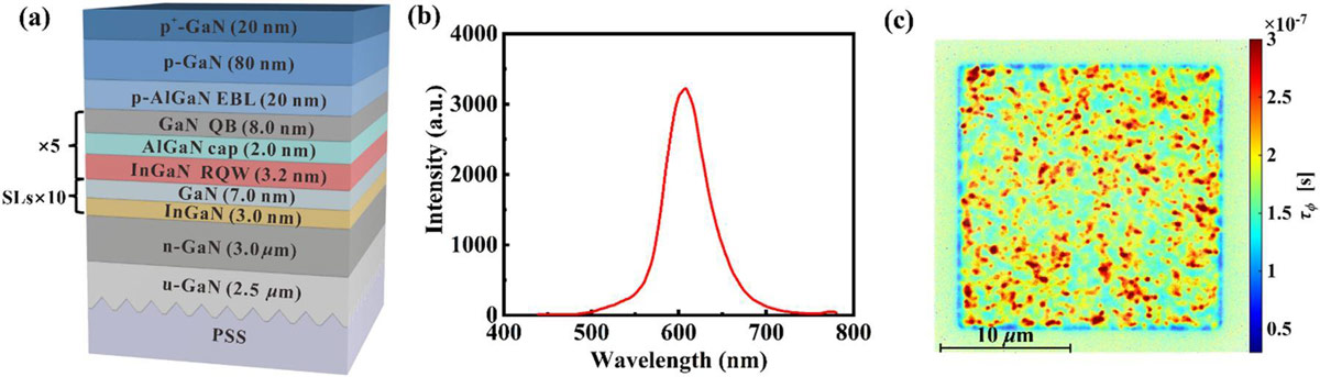
Figure 1: (a) Epitaxial structure design of nano-LED. (b) PL spectrum. (c) Fluorescence lifetime imaging microscopy (FLIM) map of amber InGaN active region.
The peak wavelength of the structure under photoluminescence was at 608nm. Fluorescence lifetime imaging microscopy (FLIM) showed strong spatial variations, suggestive of carrier localization. The team comments: “Although FLIM does not directly measure the lateral diffusion length, the observed spatial lifetime distribution suggests that carrier localization may limit effective lateral carrier transport, thereby reducing carrier capture by sidewall-related non-radiative centers in ultra-small devices.”
Circular LEDs (Figure 2) were fabricated with mesa diameter of 840nm. Indium tin oxide (ITO) was used as a 60nm current-spreading layer on the p-contact. Sidewall passivation consisted of atomic layer deposition (ALD) aluminium oxide (Al2O3) and plasma-enhanced chemical vapor deposition (MOCVD) silicon dioxide (SiO2). The chromium/titanium/gold metal electrodes were formed using electron-beam (EB) evaporation.
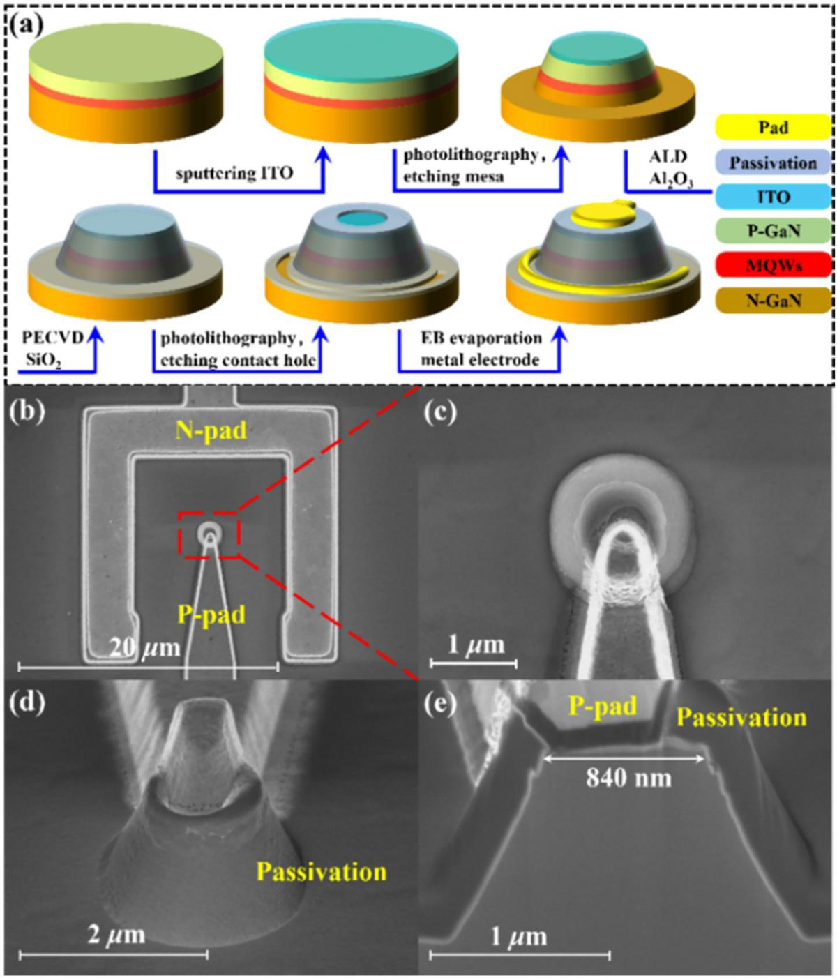
Figure 2: (a) Fabrication process. (b) Plan-view scanning electron microscope (SEM) image of complete device. (c) Enlarged SEM of central mesa. (d) Tilted-view SEM. (e) Focused ion beam (FIB) cross-section SEM.
Under 1A/cm2 current density injection the electroluminescence (EL) peak occurred at 608nm with 48nm full-width at half-maximum (FWHM). The researchers see the FWHM as being “relatively narrow compared with the EL linewidths reported for representative electrically injected broadband long-wavelength InGaN micro-/nano-LEDs.”
The EL spectrum blue-shifts 36nm to 572nm at 50A/cm2. The team views this as being the result of low-energy localized states being filled first at low injection, and then the higher-energy, shorter-wavelength states at higher currents. The higher-energy states are more typically weakly localized, and can even extended across the device.
The researchers comment: “Simultaneously, the increased carrier density screens the polarization-induced electric field and weakens the quantum-confined Stark effect. of localized-state filling, injection-induced carrier delocalization, band filling, and polarization-field screening.”
The reverse leakage current density at −5V was of order 10−6A/cm2. The team comments: “This ultralow leakage is consistent with effective suppression of defect-assisted conduction paths at the etched sidewalls by the conformal ALD-Al2O3 sidewall passivation. In addition to passivating the etched semiconductor interface, the Al2O3 layer protects the sidewalls from direct exposure to the subsequent PECVD plasma.”
The peak EQE of the 840nm-diameter LED reached 10.1% at 12A/cm2 injection (Figure 3). A larger 20μm-diameter only reached 9.8% EQE at 4A/cm2. The researchers attribute the higher EQE for the smaller device to size-enhanced light-extraction efficiency (LEE) and strong carrier localization. Simulations suggest that the 840nm device could have an LEE as high as 80%. The enhanced LEE compensates an increased tendency in the smaller device to non-radiative recombination at the sidewalls.
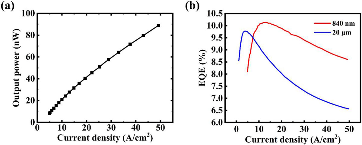
Figure 3: (a) Output power versus current density for 840nm LED. (b) EQE versus current density for 840nm- and 20μm-diameter devices.
The researchers add: “An additional contribution to the higher EQE of the ultra-small device may arise from stronger edge strain relaxation in the reduced mesa, which can weaken the strain-induced piezoelectric field, partially alleviate the quantum-confined Stark effect (QCSE), and improve the efficiency.”
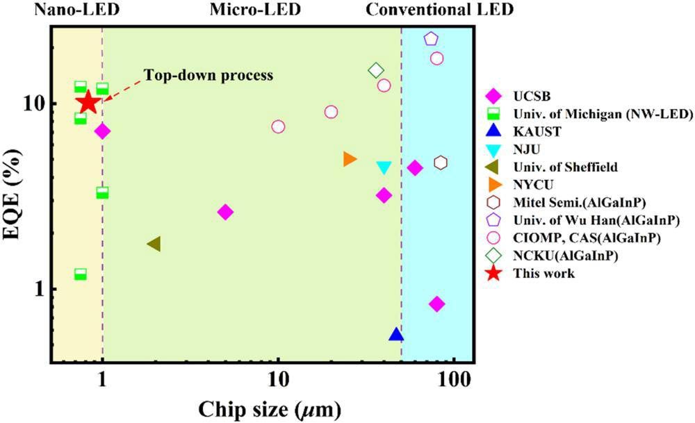
Figure 4: Benchmark plot of EQE versus chip size for reported red micro-LEDs.
The researchers compare their work against a range of LED types, including phosphide rather than III−N devices, and bottom-up nanowire (NW) structures (Figure 4). The researchers’ top-down fabricated LED is competitive with the reported nanowire LEDs.
https://doi.org/10.1063/5.0344152
The author Mike Cooke is a freelance technology journalist who has worked in the semiconductor and advanced technology sectors since 1997.