


News: Microelectronics
6 July 2020
Fraunhofer IAF embeds GaN power ICs as half-bridge in PCBs
Energy-efficient power electronics for energy conversion and transmission are becoming increasingly important, as future-oriented and sustainable energy concepts (such as electric mobility or power supply via renewable energies) depend on them. Fraunhofer Institute for Applied Solid State Physics (IAF) of Freiburg, Germany has hence developed a user-friendly, highly integrated gallium nitride (GaN) voltage converter in a compact package that is extremely resource-efficient and can be used in a modular fashion.
For years, power semiconductors have been used in voltage converters to meet the increasing demands on energy supply and usage. However, it is not only the semiconductor materials themselves that are decisive but also the packaging and design of the components because, the more compact and efficient the packaging is, the more resource-efficiently they work. However, a compact system design is often difficult to reconcile with the discrete standard components that dominate the GaN power electronics market. Most of the time, the critical conductor loops between transistors and power supply have to be individually designed and wired as circuits from discrete components.
As a user-friendly alternative, scientists at Fraunhofer IAF have embedded their GaN-based integrated power circuits (GaN power ICs) as a half-bridge in a printed circuit board (PCB), which features all critical wiring, including gate and DC link capacitors, within the package. The result is an extremely compact and efficient voltage converter suited for all 600V applications. It allows a reliable and modular system design, thus facilitating design and production processes.
Monolithically integrated GaN power ICs
Fraunhofer IAF has many years of experience in the monolithic integration of power electronic GaN chip technologies. Last year, in the course of the project GaNIAL (‘Integrated and efficient power electronics based on gallium nitride’), the researchers managed to monolithically integrate current and temperature sensors, 600V power transistors, freewheeling diodes and gate drivers in a single GaN power IC. GaN was deposited on low-cost silicon substrate (GaN-on-Si), making the chip technology suitable for cost-efficient mass production.
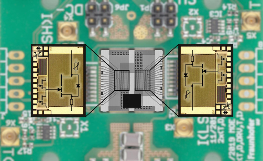
Picture: X-ray image of half-bridge circuit and circuit diagram of the integrated GaN Power ICs.
The high integration density of the GaN power ICs not only enables a higher switching frequency and therefore a higher performance density than comparable circuits but also higher reliability and compactness due to the integrated sensor technology. With their GaN power ICs in a half-bridge circuit, Fraunhofer IAF has already achieved DC-DC efficiencies of over 98.8% at 350V, and demonstrated a high switching frequency of 40MHz in continuous operation at 250V and resonant operation.
Highly integrated half-bridge circuits via PCB embedding
“GaN-on-Si technology allows monolithically integrated circuits for half-bridge converters, but does not solve the wiring problem to external capacitors. However, these critical connections to gate drivers and DC link capacitors are essential for clean and efficient switching behaviour,” Fraunhofer IAF researcher Stefan Mönch. “With our goal of a perfect voltage converter in mind, we were looking to find the optimal highly integrated packaging technology for our GaN power ICs.” For this purpose, Mönch and his team processed their ICs with a thick copper electroplating on both sides, making them suitable for PCB embedding.
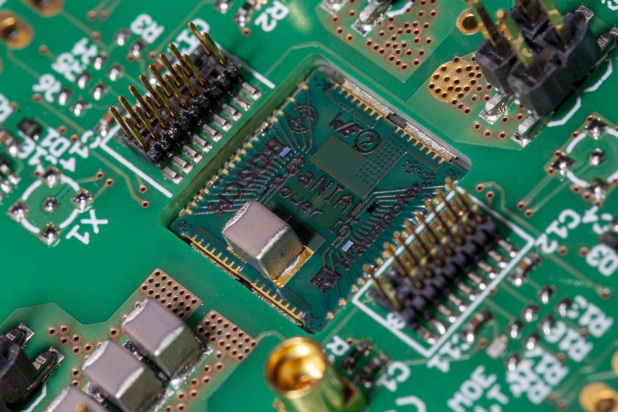
Picture: PCB-embedded GaN-on-Si half-bridge circuit including gate and DC link capacitors.
This adaptation of the metallization made it possible for the company Würth Elektronik CBT to fabricate the chips using the reliable ET Microvia Embedding Technology suitable for series production. Together with project partners Bosch and the University of Stuttgart, the researchers were able to design a PCB package that is only 12mm wide and 0.4mm flat. It integrates two monolithic GaN power ICs as a half-bridge and provides the critical decoupling capacitors for the gate driver and DC link capacitors already on the package. The embedding technology eliminates the need for bonding wires, which also minimizes parasitic inductances. The critical connections between GaN IC and capacitors are thus already optimized and no longer need to be elaborately designed by users. The result is a user-friendly solution that provides all critical components of a voltage converter already optimized in one package.
Fraunhofer IAF is presenting its latest GaN power electronics at the online PCIM (Power Conversion Intelligent Motion) Europe 2020 ‘digital days’ event (7-8 July). Fraunhofer IAF’s GaN power IC is also part of a presentation by the University of Stuttgart’s Dominik Koch at the accompanying PCIM Europe conference.
Fraunhofer IAF develops first monolithically integrated half-bridge for 600V-class
IAF GaN-on-Si GaN HEMT Power electronics


