


News: LEDs
24 July 2020
Effectively releasing tensile stress in AlN thick film for low-defect-density AlN/sapphire template
Researchers in China have demonstrated how to effectively release tensile stress in aluminium nitride (AlN) thick film by using high-temperature (HT) metal-organic chemical vapor deposition (MOCVD), permitting the growth of low-defect-density AlN/sapphire template [Chenguang He et al, ‘Fast growth of crack-free thick AlN film on sputtered AlN/sapphire by introducing high-density nano-voids’, J. Phys. D: Appl. Phys. 53 (2020) 405303]. The team hopes that this technique can enable improved performance for deep-ultraviolet light-emitting diodes (DUV LEDs).
DUV LEDs have wide application potential in water/air/surface sterilization, non-line-of-sight communication, photoionization and gas/DNA sensing. Due to the lack of large-scale and low-cost native AlN substrate, existing DUV LEDs are mainly fabricated on AlN/sapphire templates. However, the large thermal mismatch and lattice mismatch between AlN epilayers and sapphire substrates result in a high threading dislocation density (TDD). As a result, the indium-free DUV LEDs, which are extremely sensitive to TDD, have suffered from low light output power.
The researchers at China’s Guangdong Institute of Semiconductor Industrial Technology (GISIT), Guangzhou University, Peking University etc proposed to reduce TDD in an AlN/sapphire template by growing AlN thick film, which allows dislocations to climb long distances for mutual annihilation. The key to this technique is effectively releasing tensile stress in AlN thick film by introducing high-density nano-voids.
The growth of AlN film was initiated from a 20nm-thick AlN buffer sputtered on a 2-inch (0001) sapphire substrate within a NAURA iTops A230 AlN sputter system. Subsequently, the thick AlN film was fabricated on the sputtered AlN/sapphire by employing an Aixtron close-coupled showerhead (CCS) high-temperature (HT) metal-organic chemical vapor deposition (MOCVD) system. The subsequent structure consists of a 300nm-thick HT AlN-1 layer (1230°C), a 350nm-thick medium-temperature (MT) AlN interlayer (930°C), and a 4950nm-thick HT AlN-2 layer (1235°C). The total thickness of AlN film is about 5.6μm. In addition, a 5.6μm-thick AlN film without MT interlayer was also grown for comparison.
The in-situ curvature transients show that, during the growth of HT AlN-2, the rate of curvature increase of the AlN thick film with MT interlayer (Figure 1(b)) was much smaller than that of the AlN thick film without MT interlayer (Figure 1(a)), indicating much weaker tensile stress. The ultimate tensile stress intensities in the AlN thick film with MT interlayer was calculated to be 0.18GPa, demonstrating a 64% reduction compared with its counterpart without MT interlayer.
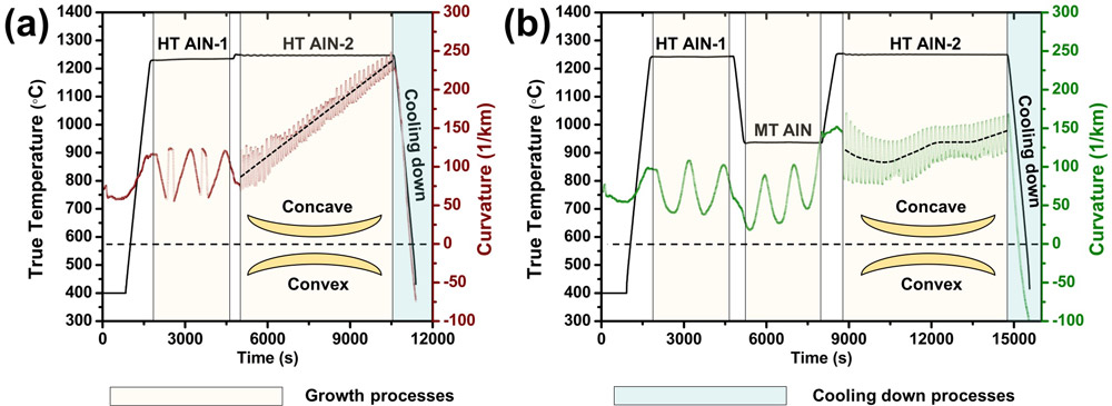
Figure 1. Curvature transients of (a) the AlN thick film without MT interlayer and (b) the AlN thick film with MT interlayer during growth and cool-down processes.
The photograph of the AlN thick film without MT interlayer (Figure 2) demonstrates that the crack-free region only accounts for 44% of the total wafer area. Cracking and peeling off took place with very high probability. In sharp contrast, the AlN thick film with MT interlayer demonstrates a mirror-like surface without any cracks except the 2mm margin. Generally, such a thick and crack-free AlN can only be obtained using the epitaxial lateral overgrowth (ELOG) technique. It further certifies that introducing an MT AlN interlayer can effectively alleviate tensile stress.
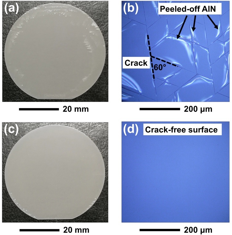
Figure 2. Photographs of (a) the AlN thick film without MT interlayer and (c) the AlN thick film with MT interlayer. Optical images of (b) the AlN thick film without MT interlayer and (d) the AlN thick film with MT interlayer.
The cross-sectional scanning transmission electron microscope (STEM) morphology images in Figure 3 show that the introduction of the MT interlayer induced the generation of high-density (1.7x1010cm-2) nano-voids, which are 40-700nm long and 10-90nm wide. These nano-voids are believed to effectively destroy the coherence between the MT interlayer and the subsequent epilayer by reducing contact area, contributing to the significantly reduced tensile stress.
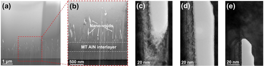
Figure 3. (a) Cross-sectional STEM morphology image of the AlN thick film with MT interlayer. (b) The enlarged cross-sectional morphology image of the red dashed area. Morphology images of a typical nano-void in the (c) bottom, (d) middle, and (e) top areas.
High-resolution x-ray diffraction (HR-XRD) measurement shows that the crystalline quality of AlN film with MT interlayer is also significantly improved. The FWHMs of (002) and (102) reflections for the AlN thick film without MT interlayer are 94 arcsec and 382 arcsec, respectively. Although the FWHM of the (002) reflection for the AlN thick film with MT interlayer slightly increases to 122 arcsec, the FWHM of the (102) reflection decreases dramatically to 196 arcsec. Cross-sectional STEM reveals that nano-voids in the AlN thick film with MT interlayer can induce dislocation termination, and nearly no new dislocations are generated at the coalescence boundaries owing to the large length-width ratios of the voids. Furthermore, during the subsequent growth process, a large proportion of the residual dislocations in sample B experience a 90° bending. Finally, the TDD of the AlN thick film with MT interlayer is reduced to an extremely low value of 4.7x107cm-2.
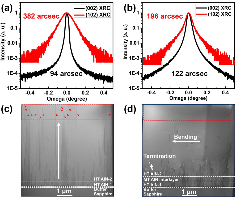
Figure 4. X-ray rocking curve scans of (002) and (102) reflections for (a) the AlN thick film without MT interlayer and (b) the AlN thick film with MT interlayer. Cross-sectional STEM images of (c) the AlN thick film without MT interlayer and (d) the AlN thick film with MT interlayer.
The researchers reckon that this technique paves the way for achieving high-performance DUV LEDs and other AlN-based optoelectronic/electronic devices.
GISIT reports low threading-dislocation-density heteroepitaxial AlN film on sapphire


