


News: Microelectronics
21 July 2022
LPE and A*STAR’s IME to develop high-quality 200mm SiC and specialty epitaxy processes
LPE SpA of Milan, Italy, which designs and makes epitaxial reactors for power electronics applications, and the Institute of Microelectronics (IME) at the Agency for Science, Technology and Research (A*STAR) have announced a research collaboration to develop high-quality 200mm silicon carbide (SiC) and specialty epitaxy processes including enhanced growth rates with improved uniformity. This will be done through experimental activities supported by simulation studies.
The parties will leverage LPE’s knowledge in SiC chemical vapor deposition (CVD) reactor technology and SiC epitaxial growth, plus IME’s research capabilities and facilities, 200mm SiC pilot process integration line, and material characterization equipment. The aim is to create 200mm epitaxy processes with enhanced growth rate and uniformities, and reduced killer defect densities.
The 200mm SiC pilot line is being established by A*STAR’s IME to validate 200mm manufacturing processes and tools on a pilot scale before transitioning to 200mm high-volume manufacturing. This collaboration will be part of IME’s plans for establishing a 200mm SiC innovation program.
SiC epitaxy is one of the essential process steps for 200mm device processing of the upcoming 200mm SiC pilot line. The manufacturing industry is projected to move towards using a unique single-wafer chamber SiC epitaxy tool. LPE, which contributes its tools into the innovation program, is geared towards quicker industrial adoption.
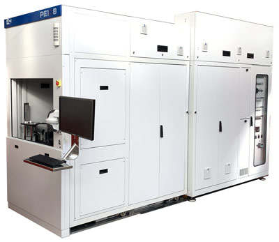 Picture: LPE’s PE1O8 SiC epitaxy reactor (photo courtesy of LPE).
For this collaboration, both parties will work on the development of high-quality 200mm SiC and specialty epitaxy processes, including the following areas:
- validation of the LPE PE1O8 SiC epitaxy reactor for 150mm/200mm wafers;
- enhancement of 200mm SiC epilayer uniformity;
- development of 200mm SiC epitaxy processes with increased growth rates;
- development of specialty SiC epitaxy processes on 200mm SiC wafers.
The collaboration will result in “extraordinary market expansion of 200mm SiC-based devices, believes LPE’s CEO Franco Preti. “As SiC power modules become pervasive, a more efficient use of electrical power will make a sustainable growth possible,” he adds.
“The success of this collaboration will benefit the SiC manufacturing ecosystem and accelerate the adoption of high-performance SiC power modules across various applications such as electric vehicles and charging points,” says IME’s executive director Terence Gan.
A*STAR’s IME and Soitec to co-develop silicon carbide for EVs and high-voltage electronics
ST and A*STAR’s IME team on silicon carbide R&D for automotive and industrial power electronics
Ascatron and LPE cooperate on 150mm SiC epitaxy for power electronics


