News: Microelectronics
18 December 2024
Fraunhofer IAF gains €4.35m from Baden-Württemberg to contribute to EU Chips Act-funded APECS pilot line
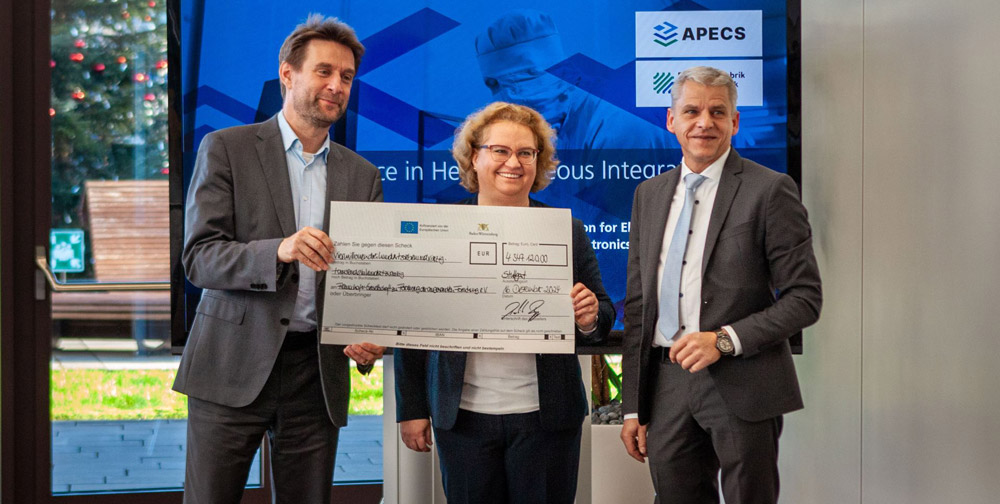
The Fraunhofer Institute for Applied Solid State Physics IAF of Freiburg, Germany says that, as part of the pilot line ‘Advanced Packaging and Heterogeneous Integration for Electronic Components and Systems’ (APECS), it will continue to expand its semiconductor research infrastructure in the coming years, supported by national funding of €4.35m via the state of Baden-Württemberg. A cheque was symbolically handed over in a visit on 16 December by Dr Patrick Rapp, the Minister for Economic Affairs, Labour and Tourism.

Picture: State Secretary Dr Patrick Rapp, Ministry of Economic Affairs, Labour and Tourism, hands over the symbolic cheque for €4.35m to Dr Patricie Merkert and professor Rüdiger Quay of Fraunhofer IAF. (photo © Fraunhofer IAF).
Also, Rapp was informed about the planned measures and the APECS pilot line, which will be coordinated by the Fraunhofer-Gesellschaft and implemented by the Research Fab Microelectronics Germany (FMD) over the next 4.5 years. APECS will make it possible to further expand the R&D infrastructure across Europe. Total funding of €730m is provided by Chips Joint Undertaking, Germany’s Federal Ministry of Education and Research (BMBF) and other funding.
“The APECS pilot line is a project of strategic importance for Baden-Württemberg, as it is about participating in highly innovative developments in the field of semiconductor technologies and supporting a rapid transfer to our companies,” said Rapp.
APECS: Heterogeneously integrated technologies
The APECS pilot line is an important component of the EU Chips Act to drive chiplet innovation and increase research and manufacturing capacity for semiconductors in Europe. The institutes cooperating in the FMD are working closely with other European partners to set up the pilot line and are thus helping to strengthen Europe’s technological resilience and boost global competitiveness in the semiconductor industry.
The pilot line will provide large industrial companies as well as small- and medium-sized enterprises (SMEs) and start-ups with low-threshold access to cutting-edge technologies and ensure secure, resilient semiconductor value chains. APECS is co-funded by Chips Joint Undertaking and by national funding from Austria, Belgium, Finland, France, Germany, Greece, Portugal and Spain under the Chips for Europe initiative. Total funding for the APECS pilot line is €730m over 4.5 years.
The APECS pilot line focuses on the scalable industrial transfer of newly developed innovations in heterointegration, in particular the use of new chiplet technologies, thus building a bridge to application-oriented research. APECS goes beyond conventional system-in-package (SiP) methods and aims to deliver robust and trustworthy heterogeneous systems that significantly increase the innovative capacity of the European semiconductor industry.
Chiplets for high-frequency applications and production on 6” wafers
As an institute cooperating in the FMD, Fraunhofer IAF is developing novel chiplets based on the hybrid material systems indium gallium arsenide-on-silicon (InGaAs-on-Si) and gallium nitride-on-silicon carbide (GaN-on-SiC) as well as micro-bump interposers as part of APECS. These technologies are particularly suitable for high-frequency applications due to their outstanding values in key parameters such as noise, output power and efficiency and promise innovations in measurement technology, communication, radar technology and sensor technology.
“Chiplets offer significant advantages in the development and production of high-performance electronic and optical components, as they enable compact and highly efficient multi-functional systems,” says Dr Patrick Waltereit, head of Fraunhofer IAF’s Technology department. “The combination of different functions such as control logic and amplifiers on one carrier improves both the performance and energy efficiency of a system.”

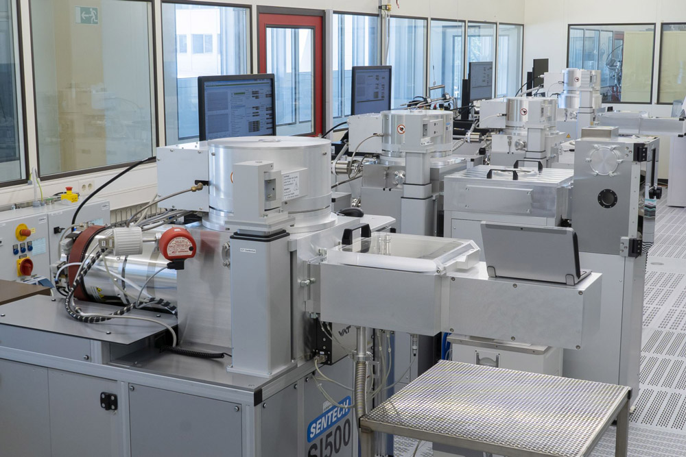
Picture: As part of the APECS pilot line, the dry etching technology area in the Fraunhofer IAF cleanroom for 6” wafers is being expanded. (photo © Fraunhofer IAF).
To ensure easy transfer to industry, the development and production of the chiplets and interposers at Fraunhofer IAF will take place on 6” wafers. New equipment for epitaxy, process technology and metrology will therefore be procured and put into operation in the institute's cleanroom. In addition, existing processes for chiplet and interposer production are being adapted.


