


News: Optoelectronics
17 April 2026
Nano-ridge surface-emitting lasers on 300mm silicon
Ghent University and imec in Belgium have reported the fabrication of one-dimensional photonic crystal nano-ridge surface emitting lasers (NRSELs) epitaxially grown on a standard 300mm silicon (Si) wafer, claimed to be the first experimental demonstration of such devices [Eslam M. B. Fahmy et al., Light: Science & Applications, v15, p120, 2006].
The Ghent–imec team have previously reported electrically pumped nano-ridge edge-emitting laser diodes, also produced on 300mm silicon [see Semiconductor Today report]. Vertical-cavity surface-emitting lasers (VCSELs) are widely used in datacom, spectroscopy and distance/position-sensing applications, e.g. in computer mice and smartphones.
VCSELs are quite complicated to fabricate, while the Ghent–imec NRSEL scheme is relatively simple. However, this first report is limited to optical pumping, and the team admits that arranging electrical contacts without blocking the emissions could be tricky.
The researchers see the direct integration on standard silicon as potentially leading to other photonic or even electronic devices. The spectral range could be shifted from around 980nm to other wavelengths by varying the indium gallium arsenide (InGaAs) composition of the active region or by using a different semiconductor family, such as the antimony-based GaSb.
The nano-ridges of III–V material (Figure 1) were grown on 300mm-diameter (001) Si wafers using an aspect ratio trapping (ART) strategy. In the first step, silicon fins in silicon dioxide (SiO2) were realized from a shallow trench isolation process. The fins were etched with tetra-methylammonium hydroxide to expose two {111} facets of the silicon crystal structure at the bottom of the etching. The {111} planes are favored for the III–V growth to avoid defects such as anti-phase disorder.
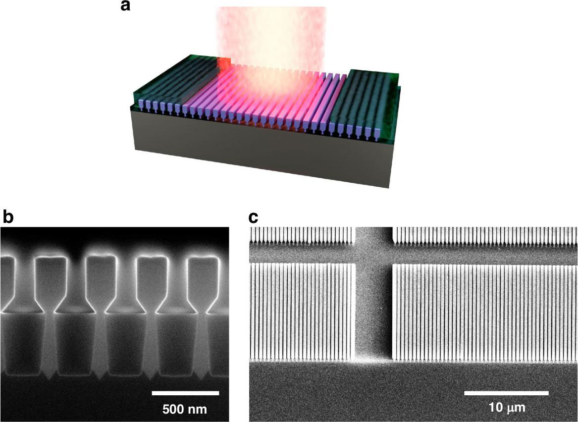
Figure 1: a NRSEL system. b Scanning electron microscope (SEM) cross section of cleaved array of nano-ridges. c Top-view SEM image of arrays of nano-ridges on silicon wafer
Metal-organic vapor phase epitaxy (MOVPE) was deployed to grow the III–V ridges consisting of three indium gallium arsenide (In0.23Ga0.77As) quantum wells (QWs) in GaAs barrier material. Once the grown material emerged from the trenches, careful growth control enabled a box shape to be maintained. The wells were 11nm thick. The structure was capped with lattice-matched indium gallium phosphide (InGaP).
The nano-ridge arrays were fabricated in 5mmx5mm blocks. The ridge period matching the gain bandwidth of the 410nm-high, 197-wide nano-ridges was 380nm (Figure 2).
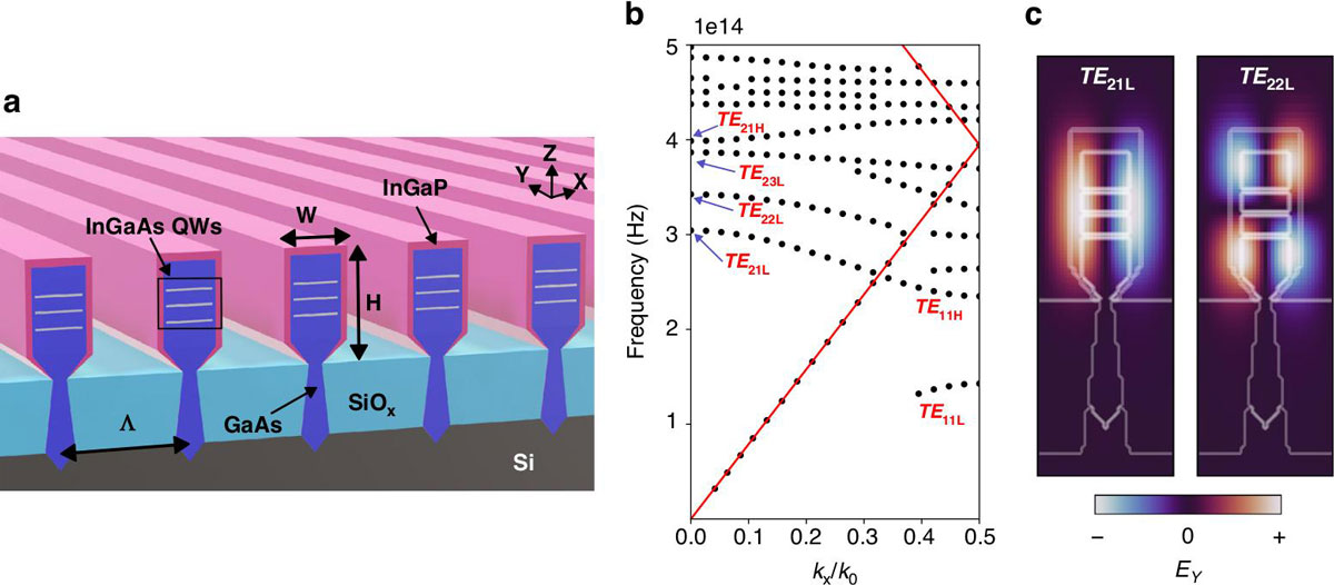
Figure 2: a Schematic array of nano-ridges with most relevant dimensional parameters. b Dispersion diagram from 2D-FDTD. Radiation continuum above light line (red). c Calculated electric field for first two band edge modes at Γ point (kx/k0=0).
Simulations were used to design the 1D photonic crystal structure. The electric field direction of the trapped bound states in the continuum (BIC) modes were designed to be near parallel with the ridge structure, parallel with the QWs. “It is well-known that the compressively strained InGaAs QWs embedded within the GaAs nano-ridges provide the highest gain for this polarization,” the researchers comment.
The finite size of the real-world devices inevitably leads to leakages away from the cavity, hopefully in the desired surface-emitting direction.
The blocks for the NRSELs were patterned and then etched using inductively coupled plasma.
Lateral confinement was provided by spin coating photoresist that filled the ridge array in the mirror sections (Figure 3). Optical lithography was used to pattern the NRSEL region for removal. The effect of the photoresist was to shift the band structure to longer wavelengths due to the 1.6 refractive index (n), compared with the near 1 value for air. The cavity mode is thus placed in a bandgap of the confinement structures, giving a mirroring effect. The mirror regions were 15µm wide.
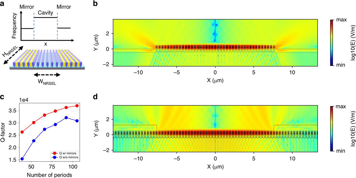
Figure 3: a Side mirrors defined by locally shifting slow trapped Bloch mode to longer wavelength. b, d 2D-FDTD simulations of finite nano-ridge crystal without and with mirrors, respectively. c Calculated Q-factor for TE21L mode without and with side mirrors, as a function of number of periods.
The optical pumping was through a nanosecond-pulsed 532nm wavelength 300µm-diameter spot from a Nd:YAG laser.
The laser emission wavelength was around 984nm for a device with a 20µm-wide, 15µm-high cavity. The narrowest linewidth was 0.9nm, measured just above threshold. “We believe the linewidth to be limited by the pulsed optical pumping,” the researchers report.
The researchers studied the effect of varying the cavity width on the threshold (Figure 4). The leveling off of the threshold reduction with width is attributed to the saturation of the Q-factor enhancement expected, based on 2D finite difference time-domain (FDTD) simulations.
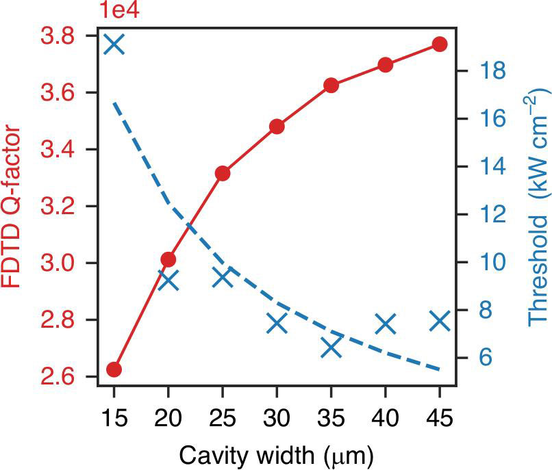
Figure 4: Mean laser threshold data and Q-factor calculated from 2D-FDTD simulation, along with a/W+b fit, versus cavity width (W).
The researchers comment: “The saturation of the threshold might indicate the influence of random disorder effects, as longer-cavity photonic crystal lasers tend to suffer higher losses (often referred to as slow-light induced losses) when operating near the band-edge. Notably, the minimum lasing threshold was found for devices with a 35μm cavity, which also exhibited the smallest spread in threshold values—suggesting that the optimal cavity dimension minimizes the impact of fabrication-induced disorder.”
One-dimensional photonic crystal nano-ridge surface emitting lasers NRSELs InGaAs InGaP GaAs MOVPE
https://doi.org/10.1038/s41377-025-02061-z
The author Mike Cooke is a freelance technology journalist who has worked in the semiconductor and advanced technology sectors since 1997.


