


News: LEDs
15 December 2020
Aledia produces first micro-LED chips on 300mm silicon wafers
Aledia S.A of Echirolles, near Grenoble, France (a developer and manufacturer of 3D micro-LEDs for display applications based on its gallium nitride nanowires-on-silicon platform) has manufactured what is says are the first micro-LED chips produced on 300mm (12”) silicon wafers.
The firm, which developed its technology on 200mm (8”) silicon wafers over the past eight years, will produce the chips on both 200mm and 300mm wafers. The larger wafers provide better economic payoff and cost-effective integration with smaller-node electronics, which are only available on 300mm silicon wafers. Aledia was spun out of Grenoble-based micro/nanotechnology R&D center CEA-Leti in 2012, and the work on 300mm wafers has been performed by joint Aledia and CEA-Leti teams.
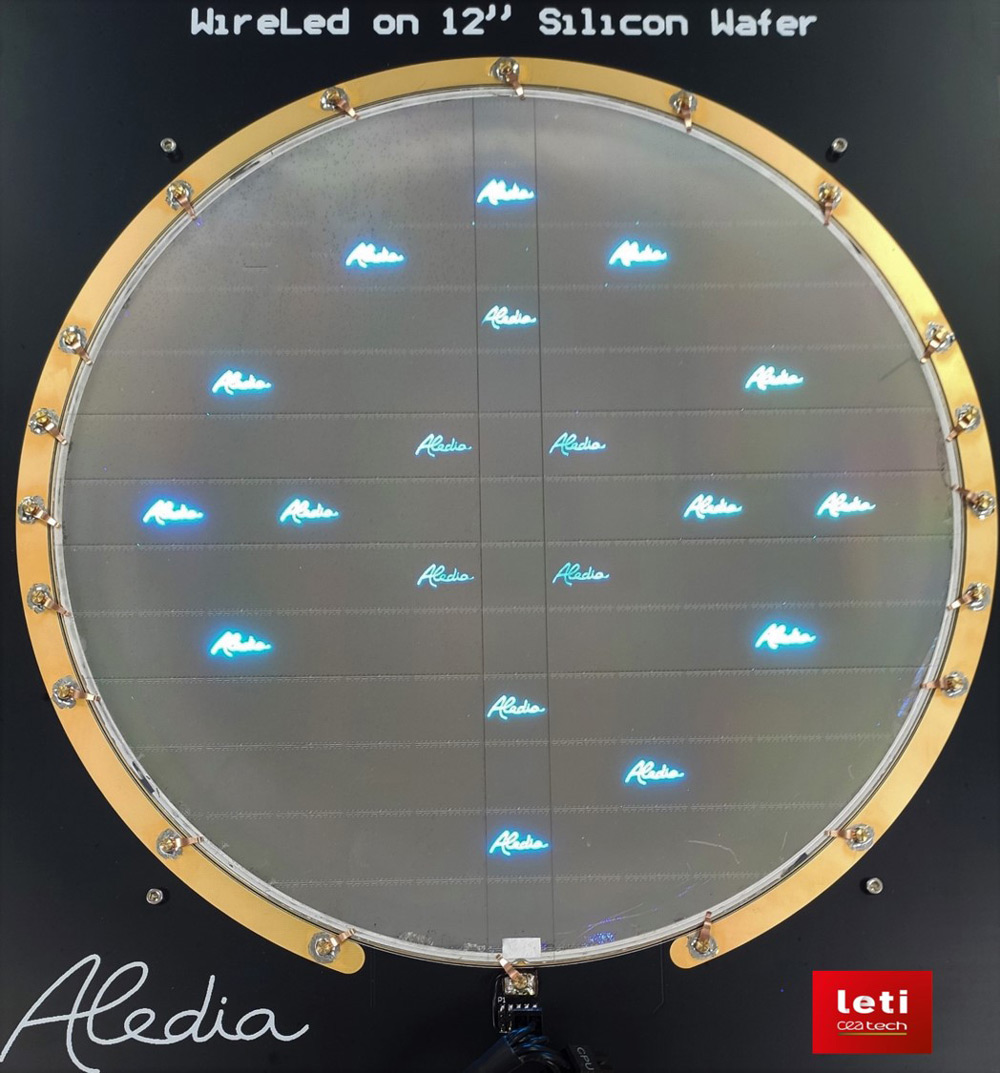
“Producing micro-LEDs on large-area 300mm silicon wafers is a world’s first, and opens this technology to huge potential-volume-manufacturing capabilities,” believes CEO & co-founder Giorgio Anania. “The larger size allows 60-100 smartphone displays to be made on a single 300mm wafer, versus approximately four-to-six using the present LED industry-standard, 4” sapphire substrate,” he adds. “Thanks to Aledia’s unique nanowire LED technology (3D LED), this can be done with commercially available processes and equipment, since it uses standard-thickness (780µm) silicon wafers.”
Traditional planar 2D micro-LEDs are produced by depositing layers of GaN crystal on sapphire wafers of 100-150mm (4-6”) diameter, with most production currently being on 100mm (4”) wafers. Aledia’s micro-LED technology grows GaN nanowires on top of large-area silicon. This 3D nanowire technology does not create any of the stresses seen on 2D chips, which build up as the wafer size is increased, and so allows the use of very large-size wafers, says Aledia. In addition, the silicon-based technology allows production in conventional foundries, which can be ramped up to high-volume production with extremely high yield.
“We are very pleased to have helped Aledia push forward the state of the art of 3D LED manufacturing using our 300mm silicon processing line. We believe large-area silicon wafers are the best manufacturing platform in the world today for displays, and give big advantages in manufacturability,” says CEA-Leti’s CEO Emmanuel Sabonnadière. “3D nanowire micro-LEDs have the potential to make serious penetration into large-display markets. CEA-Leti is very active today in supporting the display industry’s transition to micro-LED technology,” he adds.
“The use of large-area silicon wafers and microelectronics foundries are the only way to deliver the huge volumes demanded by end-user markets,” believes Anania. “For example, if only the large-screen TVs of 60” in diagonal and larger transitioned to silicon nanowire technology to obtain better image quality and lower manufacturing costs, this would require 24 million 300mm wafers per year, volumes that can only be delivered by the silicon industry and supply chains. Smartphones, laptops and tablets would be on top of that.”
Aledia’s technology is protected by 197 patent families, making it the leading French startup company in France in filed patents, it is reckoned.
The work is sponsored by the European Commission (EC) Horizon 2020 grant agreement 954553 for the project SPEED (‘Smart Pixel Emitters For Display’ — H2020-EIC-SMEInst-2018-2020), which runs from 1 August 2020 to 31 July 2022.
Aledia chooses Veeco’s Propel 300 HVM MOCVD platform for micro-LED displays
Aledia closes €80m first tranche of €120m Series D funding round
Aledia benefits from strong patent portfolio in GaN-on-Si nanowire LEDs


