


News: Suppliers
22 September 2021
Enkris demonstrates CMOS-compatible high-voltage GaN-on-Si HEMT epi reaching 300mm
Enkris Semiconductor of Suzhou Industrial Park, China – which was founded in 2012 as a pure-play foundry for gallium nitride (GaN) epitaxial wafers for power electronics, RF, micro-LED and UVC applications – says that it has demonstrated a series of high-quality 300mm GaN-on-silicon high-electron-mobility transistor (HEMT) epiwafers of what it claims are excellent thickness uniformity and low wafer bow for 200V, 650V and 1200V power applications, paving the way for device processing using more sophisticated 300mm CMOS-compatible lines.
Advances in GaN epitaxy on large-size silicon substrates have enabled GaN-on-Si power devices with high performance and reliability by combining the full advantage of both the properties of GaN and production in a CMOS-compatible processing line, says Enkris. Commercial GaN power devices based on GaN-on-Si HEMT technology are gaining in popularity for a wide range of applications such as consumer electronics, industrial electronics and data centers, and in the energy, automotive and mobility sectors. Driven by cost reduction and more sophisticated integrated circuit design, the industry is now moving towards larger wafer sizes, notes Enkris.
Following its launch of commercial 200mm GaN-on-Si HV (high-voltage) HEMT epiwafers in 2014, Enkris has now transferred its AlGaN/GaN HEMT epitaxy process to 300mm silicon substrates, while maintaining the thickness uniformity as well as low wafer bow within 50µm. The vertical voltage breakdown measurements suggest that the wafers are suitable for 200V, 650V and 1200V power applications (see Figure 1).
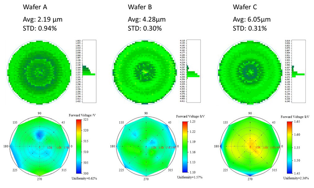
Figure 1: Thickness map and vertical breakdown voltage (leakage current = 1μA/mm2 @ RT) of a series of Enkris 300mm GaN-on-Si HEMT epiwafers targeting 200V, 650V and 1200V power applications, respectively.
The 300mm GaN-on-Si HEMT epitaxial layer structure adopted to solve the key issues of wafer cracking/bow and high crystalline defects is shown in Figure 2(a). Growth starts with an AlN nucleation layer, followed by a strain relief stack, GaN channel, AlGaN barrier and GaN cap. The narrow x-ray diffraction (XRD) AlN(002) peak and good uniformity of FWHM (full width at half maximum), as shown in Figure 2(b), indicate a high crystalline quality across the whole 300mm wafer.
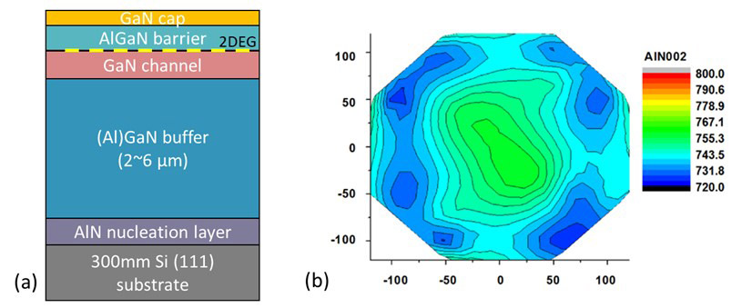
Figure 2: (a) Schematic structure of Enkris 300mm GaN-on-Si HEMT epiwafers. (b) Map of XRD AlN(002) FWHM, giving an average FWHM value of 743arcsec and a STD of 2%.
Figure 3 shows the aluminium composition in the AlGaN barrier and the two-dimensional electron gas (2DEG) carrier concentration measured at nine positions from wafer center to wafer edge. The measurements give an average value of 19.9% and a standard deviation (std) of 0.68% of Al composition in the AlGaN barrier (Figure 3a), suggesting a uniform 2DEG electrical characteristics. This has been confirmed by the capacitance-voltage (CV) measurements, revealing an average electron concentration of 7.2x1012cm-2 with a std <2% (Figure 3b).
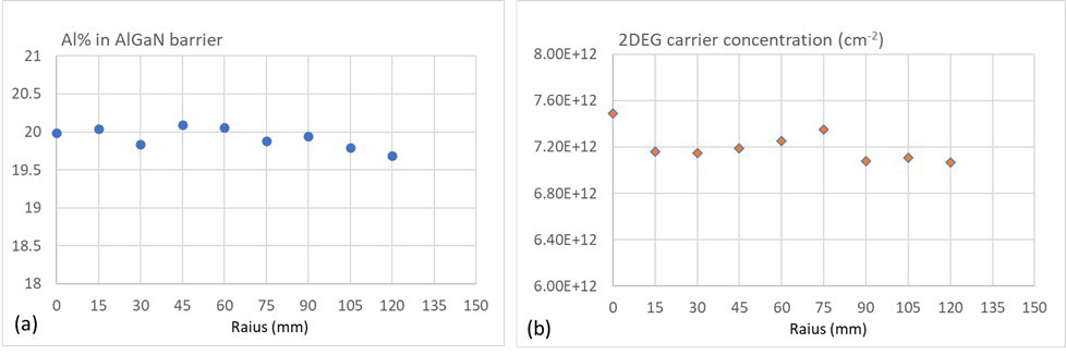
Figure 3: Al composition and 2DEG electron concentration measured from Enkris’ AlGaN/GaN HEMT epiwafer grown on 300mm silicon substrates.
“Thanks to our optimized AlN nucleation layer, we are able to produce crack-free GaN-based HEMT epiwafers that meet the leakage current requirements on large-size silicon substrates up to 300mm,” says CEO Dr Kai Cheng. “Despite the challenges in the epitaxy process, strain management and defect control when moving to 300mm wafer size, we have achieved excellent structural quality and electrical properties in the AlGaN/GaN HEMT structures. This will certainly encourage the development of high-power integrated circuits to yield system-on-chip and further reduce the cost of GaN power devices,” he reckons.
Gallium nitride complementary logic on silicon using normally-off transistors
First demonstration of fully vertical gallium nitride transistors on silicon
Platform for fully vertical gallium nitride on silicon power devices
Increasing gallium nitride MOSFET threshold voltage
Enkris uses Aixtron system to demo high-voltage GaN HEMT structures on 200mm silicon


